Semiconductor transverse device and high-voltage device

一种横向器件、高压器件的技术,应用在半导体器件、电固体器件、晶体管等方向,能够解决牺牲器件性能等问题

Inactive Publication Date: 2009-09-02
UNIV OF ELECTRONICS SCI & TECH OF CHINA
View PDF3 Cites 4 Cited by
  • Summary
  • Abstract
  • Description
  • Claims
  • Application Information

AI Technical Summary

Problems solved by technology

However, this method sacrifices the performance of the device on the one hand, and on the other hand does not essentially eliminate the electric flux distribution on the device surface caused by the conduction of a single carrier that deviates from the electric flux distribution on the device surface when there are no carriers. effect

Method used


Image

  • Semiconductor transverse device and high-voltage device
  • Semiconductor transverse device and high-voltage device
  • Semiconductor transverse device and high-voltage device

Examples


Embodiment Construction

[0057] The present invention will be described more fully hereinafter with reference to the accompanying drawings, in which exemplary embodiments of the invention are illustrated. In the drawings, the same reference numerals denote the same or similar components or elements.

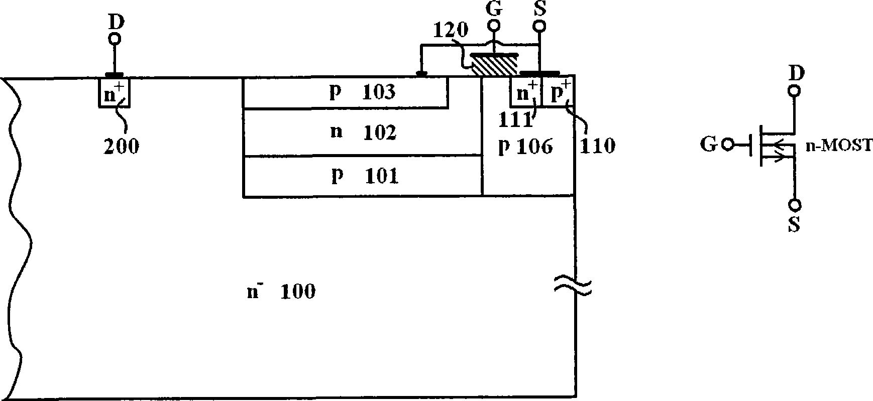
[0058] figure 1 An example of n-LDMOS fabricated using the basic withstand voltage structure in reference [4] is shown. The n-LDMOS conducts electricity only by electrons, where the electrodes D and n + The drain region 200 is connected, the electrodes S and n + source region 111 connected, and via p + Region 110 is directly associated with source substrate region p-region 106 . The electrode G is the gate electrode of the n-LDMOS, and the shaded area 120 in the figure is a gate oxide layer or a gate insulating layer. The p region 101, the n region 102 and the p region 103 constitute the surface withstand voltage region of the n-LDMOS. It is worth noting that the connection from the S pole to the p...


PUM


Abstract

The invention provides a semiconductor transverse device and a high-voltage device. The semiconductor transverse device is provided with three external connection terminals, utilizes two current carriers to conduct electricity and comprises a highest voltage area and a lowest voltage area which both take a substrate as zero-voltage, and a surface voltage resisting area is formed between the highest voltage area and the lowest voltage area. The highest voltage area and the lowest voltage area are internally provided with an external connection terminal and a control terminal respectively, wherein one control terminal is in external connection and controls one type of current carrier flow, and the other control terminal is built in and controls the other type of current carrier flow; and an electric potential on the built-in control terminal is adjusted and controlled by the external voltage of external-connection control terminal. The attached drawing in the abstract shows a method for manufacturing the devices by using an n-MOSFET to control electron current and a pnp bipolar transistor to control cavity current, wherein the electric potential of the base region of the pnp bipolar transistor is adjusted and controlled by external voltage on an n-MOSFET gate electrode.

Description

technical field [0001] The invention relates to the technical field of semiconductors, in particular to a semiconductor lateral device and a high-voltage device. Background technique [0002] As we all know, withstand voltage, specific on-resistance and reliability are extremely important parameters of power devices. [0003] High-voltage lateral power devices experience high-voltage and high-current states during switching. At this time, for a lateral power device with a single type of carrier conduction, the carriers introduced by the large current density will cause the electric flux distribution on the device surface to deviate from the electric flux distribution on the device surface when there are no carriers, making the device local The regional electric field is enhanced, and the impact ionization rate increases, which is easy to cause local avalanche breakdown. [0004] The above phenomenon has a negative impact on the reliability of the high-voltage lateral power...

Claims


Application Information

Patent Timeline
Patent Type & Authority Applications(China)
IPC IPC(8): H01L27/06H01L29/78H01L29/735H01L29/06
CPCH01L29/7393H01L29/7394H01L29/1095H01L29/7816H01L27/0716H01L29/7817H01L29/7831H01L29/0847H01L27/0738H01L29/7835H01L29/0634
Inventor 陈星弼
Owner UNIV OF ELECTRONICS SCI & TECH OF CHINA
Why Eureka
Try Eureka