Diode and manufacturing method thereof

A diode and metal anode technology, which is applied in the field of power semiconductor devices, can solve the problems of large conduction loss and poor reverse recovery characteristics, and achieve the effect of reducing the reverse recovery charge Qrr and optimizing the reverse recovery characteristics

Active Publication Date: 2018-11-02
UNIV OF ELECTRONICS SCI & TECH OF CHINA
View PDF4 Cites 2 Cited by
  • Summary
  • Abstract
  • Description
  • Claims
  • Application Information

AI Technical Summary

Problems solved by technology

[0005] In view of the foregoing, the object of the present invention is to: aim at the problems of large conduction loss and poor reverse recovery characteristics of PIN diodes in the prior art, and provide a device that can reduce the forward conduction voltage and optimize the reverse recovery characteristics. The diode device structure, the device structure is applicable to various semiconductor materials; meanwhile, the invention also provides the preparation method of the diode device

Method used


Image

  • Diode and manufacturing method thereof
  • Diode and manufacturing method thereof
  • Diode and manufacturing method thereof

Examples


Embodiment 1

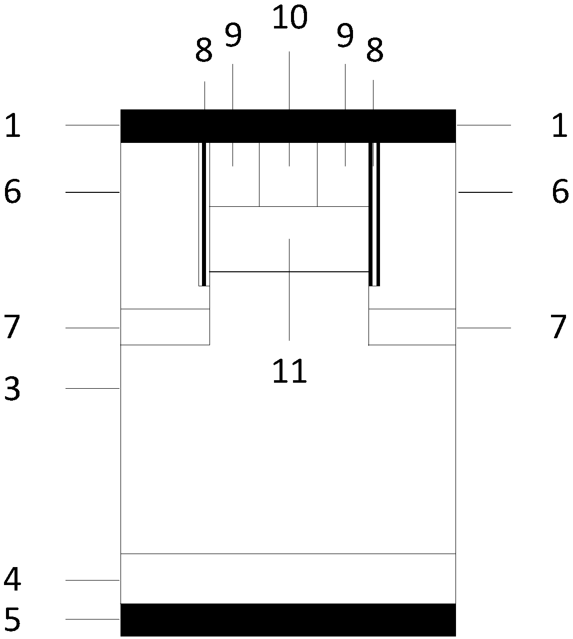
[0074] A diode device whose cell structure is as figure 2As shown, it includes metal cathode 5, N+ silicon carbide substrate 4, N- silicon carbide epitaxial layer 3 and metal anode 1 stacked in sequence from bottom to top; both sides of the top layer of N- silicon carbide epitaxial layer 3 have trench structures , the trench structure includes a P+ silicon carbide region 7 at the bottom of the trench and a polysilicon 6 at the top of the trench, the P+ silicon carbide region 7 is in direct contact with the polysilicon 6; the top layer of the N-silicon carbide epitaxial layer 3 is two There is also a P-type silicon carbide body region 11 between the trench structures on the side. The source region 9 is characterized in that: the N+ silicon carbide source region 9, the P-type silicon carbide body region 11 and part of the N- silicon carbide epitaxial layer 3 are in contact with the polysilicon 6 through the dielectric layer 8 on the side wall of the trench; the polysilicon 6 ,...

Embodiment 2

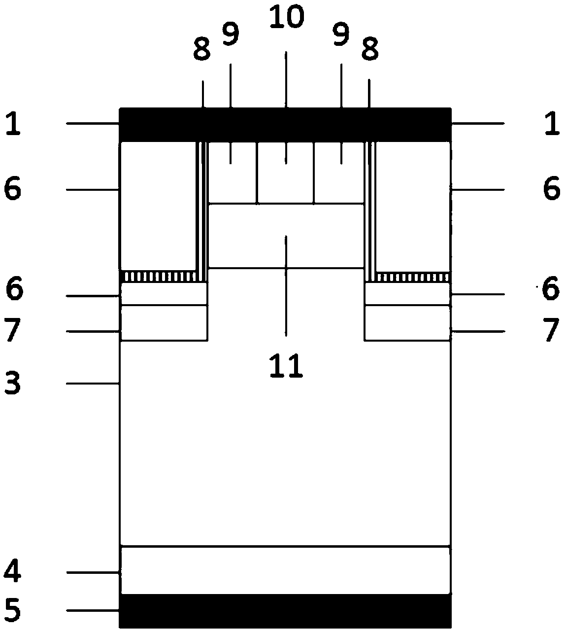
[0084] The schematic diagram of the cell structure of the diode device provided in this embodiment is as follows: image 3 As shown, the difference compared with Embodiment 1 is that the bottom end of the dielectric layer 8 extends laterally to separate the polysilicon 6 into two independent parts, and the polysilicon 6 under the dielectric layer 8 is short-circuited with the metal anode 1. The method keeps the potential of the polysilicon 6 consistent with the potential of the metal anode 1 at all times, avoiding the fluctuation of the I-V characteristic of the super-barrier structure caused by the potential change of the polysilicon 6 after the heterojunction is turned on. Compared with Embodiment 1, this embodiment improves the reliability of the device in practical applications.

Embodiment 3

[0086] The schematic diagram of the cell structure of the diode device provided in this embodiment is as follows: Figure 4 As shown, the difference compared with Embodiment 2 is that the lateral width of the P+ silicon carbide region 7 is made larger. Compared with Embodiment 2, the larger the lateral width of the P+ silicon carbide region 7 is, when the device is in the blocking state, the stronger the electric field shielding effect of the region above the P+ silicon carbide region 7 is. Structures such as heterojunction and super barrier structure also improve the withstand voltage performance of the device. It should be noted that the wider the width of the P+ silicon carbide region 7 is, the greater the on-resistance of the device works in the forward direction. Therefore, the width of the P+ silicon carbide region 7 needs to be balanced between forward and reverse operation.

[0087] In this embodiment, an N-channel diode device is taken as an example, and the width o...


PUM


Abstract

The invention discloses a diode device and a manufacturing method thereof, and belongs to the technical field of power semiconductor devices. A cellular structure of the device comprises a metal negative electrode, an N+ substrate and an N- epitaxial layer; a trench structure is arranged on the two sides of the top layer of the epitaxial layer; the trench structure comprises a P-type semiconductorregion and a heterogeneous semiconductor from the bottom up; the top layer of the N-epitaxial layer is also provided with a P-type body region, an N+ source region and a P+ contact region; the N+ source region, the P-type body region, a part of the N- epitaxial layer and the heterogeneous semiconductor are in contact through a dielectric layer of the side wall of the trench; the surface of the device is covered with a metal positive electrode; and the heterogeneous semiconductor, the dielectric layer, the source region, the body region and the epitaxial layer form an ultra-potential barrier structure. By virtue of the diode device and the manufacturing method thereof, the problems of high forward opening voltage, poor reverse recovery capability and the like existing in the existing PIN diode device can be solved; and in addition, lower electric leakage and a larger safe working region are achieved on the premise that the withstand voltage is not affected, and the reliability of the device is improved.

Description

technical field [0001] The invention belongs to the technical field of power semiconductor devices, and in particular relates to a diode and a manufacturing method thereof. Background technique [0002] According to statistics, more than 90% of the electricity consumption in the world is controlled by power devices. Power devices and their modules provide an efficient way to realize the conversion of various forms of electric energy, and have been widely used in national defense construction, transportation, industrial production, medical and health and other fields. Since the first power device application in the 1950s, each generation of power devices has enabled more efficient conversion and use of energy. The history of power semiconductor devices, that is, the history of new power semiconductor devices. [0003] Power diodes are the simplest electronic components among many power semiconductor devices, but they are also one of the most widely used devices and play a v...

Claims


Application Information

Patent Timeline
Patent Type & Authority Applications(China)
IPC IPC(8): H01L29/872H01L29/06H01L21/329
CPCH01L29/0603H01L29/0634H01L29/0684H01L29/6606H01L29/8725
Inventor 张金平邹华罗君轶刘竞秀李泽宏张波
Owner UNIV OF ELECTRONICS SCI & TECH OF CHINA
Why Eureka
Try Eureka