

A Superjunction MOSFET with Improved Reverse Recovery Characteristics
A reverse recovery and characteristic technology, applied in the direction of diodes, semiconductor devices, electrical components, etc., can solve problems such as adverse effects of application systems and increased losses
- Summary
- Abstract
- Description
- Claims
- Application Information
AI Technical Summary
Problems solved by technology
Method used
Image

Examples
Embodiment Construction
[0016] The present invention is described in detail below in conjunction with accompanying drawing
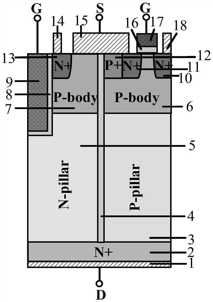
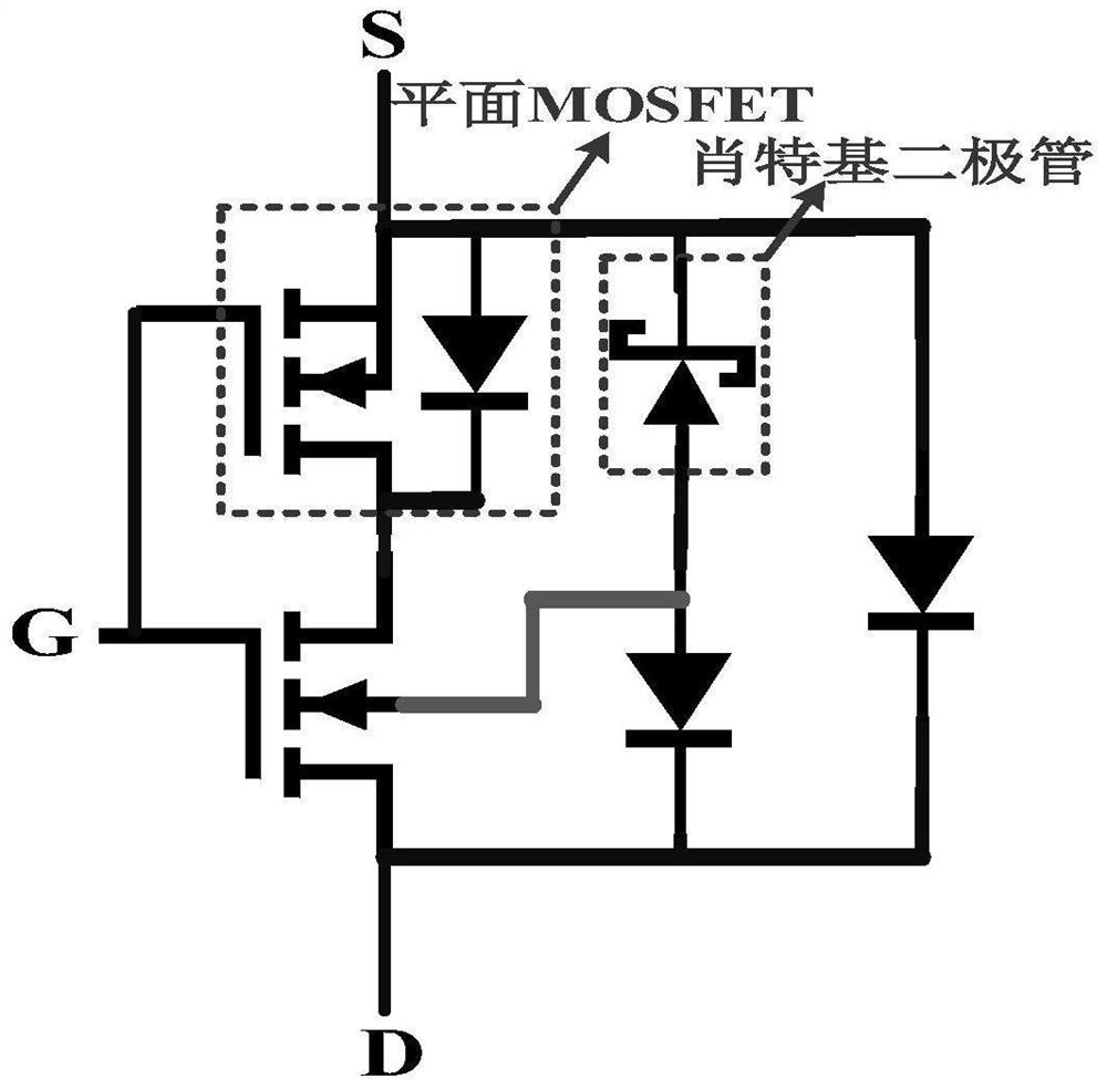
[0017] Such as figure 1 As shown, it is the super junction MOSFET with improved reverse recovery characteristics of the present invention, and the equivalent circuit diagram is as follows figure 2 shown. The source metal 15 and the first P-type well region 7 form a P-type Schottky diode, and the third insulating medium 16, the second conductive material 17, the second N+ source region 11, the second N+ drain region 10 and the P+ body contact The region 12 forms a planar MOSFET, wherein the second N+ drain region 10 is the drain, the second N+ source region 11 and the second P+ body contact region 12 are the source, and the second conductive material 17 is the gate. The gate terminal of the planar MOSFET is the gate of the device, and its second N+ drain region 10 is connected to the first floating metal through the second floating metal 18 . Compared with the conventional s...
PUM
 Abstract
Description
Claims
Application Information