Super-junction MOSFET device with improved reverse recovery characteristic

A technology of reverse recovery and devices, which is applied in the direction of semiconductor devices, electrical components, diodes, etc., can solve the problem of energy loss and achieve the effect of improving reverse recovery characteristics

Pending Publication Date: 2021-11-05
SHANGHAI DAOZHI TECH CO LTD
View PDF0 Cites 0 Cited by
  • Summary
  • Abstract
  • Description
  • Claims
  • Application Information

AI Technical Summary

Problems solved by technology

Since the superjunction MOSFET injects far more holes than the traditional MOSFET when the parasitic diode is turned on, more energy will be lost in the process of reverse recovery and extraction of excess carriers.

Method used


Image

  • Super-junction MOSFET device with improved reverse recovery characteristic
  • Super-junction MOSFET device with improved reverse recovery characteristic
  • Super-junction MOSFET device with improved reverse recovery characteristic

Examples


Embodiment Construction

[0013] In order to make those skilled in the art more clearly understand the purpose, technical solutions and advantages of the present invention, the present invention will be further described below in conjunction with the accompanying drawings and embodiments.

[0014] In describing the present invention, it should be understood that the orientations indicated by terms such as "upper", "lower", "left", "right", "inner", "outer", "transverse", "vertical" etc. Or the positional relationship is based on the orientation or positional relationship shown in the drawings, which is only for the convenience of describing the present invention, and does not indicate or imply that the referred device or element must have a specific orientation, so it should not be construed as a limitation of the present invention.

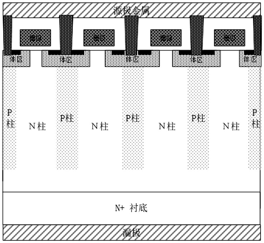
[0015] refer to figure 1 as shown, figure 1 It is the cross-section of the existing super junction MOSFET device. The parasitic diode is formed by the P-type body region...


PUM


Abstract

The invention discloses a super-junction MOSFET device with an improved reverse recovery characteristic, which comprises an N + substrate layer and a plurality of P columns and N columns which are alternately arranged on the N + substrate layer. A drain electrode is arranged at the bottom of the N + substrate layer; the top of the P column and the top of the N column are provided with an N epitaxial layer, the N epitaxial layer is provided with P-type body regions corresponding to the P columns in position and number, the P columns in a partial region in the super-junction MOSFET device body extend upwards to form epitaxial P columns, and the epitaxial P columns penetrate through the N epitaxial layer and are connected with the P-type body regions at the corresponding positions so as to maintain the same potential; and a dielectric layer is arranged at the tops of the P-type body regions, a source metal layer and a first metal layer which respectively correspond to the positions of the P columns and the epitaxial P columns are arranged at the top of the dielectric layer, a plurality of connecting holes are formed in the dielectric layer, and at least one diode is connected in series between the epitaxial P column and the source metal layer of the primitive cell in a forward direction or a reverse direction.

Description

technical field [0001] The invention relates to the field of design and process manufacturing of super junction MOSFET (SJ-MOSFET) devices, in particular to a super junction MOSFET device with improved reverse recovery characteristics. Background technique [0002] The basic structure of a super junction MOSFET device is composed of alternately arranged P columns and N columns. When the device is in the blocking state, the P and N columns in the superjunction structure are completely depleted, and the longitudinal electric field of the device tends to be uniformly distributed under the modulation of the lateral electric field in the drift region. Theoretically, the withstand voltage capability of the super-junction structure depends only on the thickness of the drift region, and has nothing to do with the doping concentration. Therefore, the super-junction structure breaks the "silicon limit" that the on-resistance of traditional power devices is limited by the breakdown vol...

Claims


Application Information

Patent Timeline
Patent Type & Authority Applications(China)
IPC IPC(8): H01L29/78H01L29/06
CPCH01L29/7805H01L29/0634H01L29/0684H01L29/7811
Inventor 陈雪萌王艳颖钱晓霞汤艺
Owner SHANGHAI DAOZHI TECH CO LTD
Why Eureka
Try Eureka