Unidirectional transient suppression diode and preparation process thereof

A technology of transient suppression and preparation process, applied in semiconductor/solid-state device manufacturing, semiconductor devices, electrical components, etc., can solve the problems of unstable breakdown voltage, increased cost, TVS reliability easily affected by charges, etc., to achieve Effect of improving negative surge capability

Pending Publication Date: 2022-02-08
WILL SEMICON (SHANGHAI) CO LTD
View PDF0 Cites 0 Cited by
  • Summary
  • Abstract
  • Description
  • Claims
  • Application Information

AI Technical Summary

Problems solved by technology

[0003] As the application environment becomes more and more complex, the circuit has higher and higher requirements for anti-surge capability. In order to improve the surge capability, the area of ​​the protection device can be increased, but the cost will increase. As the integration level becomes higher and higher, the surge The area of ​​protection devices is getting smaller and smaller, so it becomes more important to improve the surge capability without increasing the area
[0004] At the same time, TVS reliability is highly susceptible to charge
The instability of the breakdown voltage will cause many problems in practical applications

Method used


Image

  • Unidirectional transient suppression diode and preparation process thereof
  • Unidirectional transient suppression diode and preparation process thereof
  • Unidirectional transient suppression diode and preparation process thereof

Examples


Embodiment 1

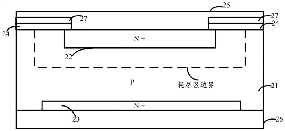
[0040] Such as figure 2 As shown, the embodiment of the present application provides a unidirectional TVS diode, including a substrate 21 of a first conductivity type, a first injection region 22 and a second injection region 23 of a second conductivity type;

[0041] The first implantation region 22 is arranged on the front side of the substrate 21, and the second implantation region 23 is arranged on the backside of the substrate 21, wherein the junction depth of the pn junction formed between the second implantation region 23 and the substrate 21 is smaller than that between the first implantation region 22 and the substrate 21. The junction depth of the pn junction formed between the substrates 21 is provided with a barrier layer 24 and an insulating layer 27 sequentially from bottom to top on the front surface of the substrate 21; the first injection region 22 draws out the first electrode through the first metal 25, The insulating layer 27 is arranged between the barrie...

Embodiment 2

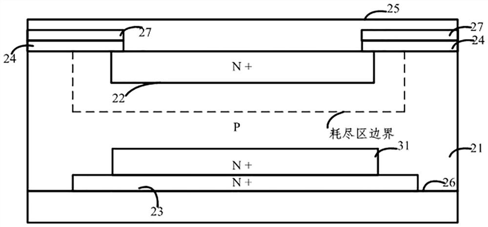
[0045] On the basis of Example 1, such as image 3 As shown, the diode provided by the embodiment of the present application also includes a third implantation region 31 of the second conductivity type, the second implantation region 23 is larger than the width of the third implantation region 31, and the second implantation region 23 on the back side is set to be third than the front side of the substrate. The reason why the first injection region 22 is wide is that the second injection region 23 on the back side is an electron emission region, and the quantity of electron emission is related to the area. The larger the area, the more electrons are emitted, and the stronger its flow capacity is. In the embodiment of the present application, the first The junction depth of the pn junction formed between the third implant region 31 and the substrate 21 is greater than the junction depth of the pn junction formed between the first implant region 22 and the substrate 21, and the s...

Embodiment 3

[0048] On the basis of Example 3, as Figure 4 As shown, the unidirectional TVS diode provided by the embodiment of the present application further includes a fourth injection region 42 of the first conductivity type and / or a fifth injection region 41 of the second conductivity type; the fifth injection region 41 covers the first An injection region 22, the fifth injection region 41 is separated from the first injection region 22 by a preset distance, and the boundary of the depletion region on the surface can be extended gently by the distance between the fifth injection region 41 and the first injection region 22. The fourth injection region 42 covers the second injection region 23, The fourth implantation region 42 is in contact with the second implantation region 23, and the fourth implantation region 42 is in contact with the second implantation region 23 on the back side of the substrate to form a pn between the fourth implantation region 42 and the second implantation re...


PUM


Abstract

The invention discloses a unidirectional transient suppression diode and a preparation process thereof. The diode comprises a substrate of a first conduction type, a first injection region of a second conduction type, and a second injection region of the second conduction type. The first injection region is arranged on the front face of the substrate, the second injection region is arranged on the back face of the substrate, and the junction depth of a pn junction formed between the second injection region and the substrate is smaller than that of a pn junction formed between the first injection region and the substrate. A barrier layer and an insulating layer are sequentially arranged on the front surface of the substrate from bottom to top; a first electrode is led out from the first injection region through first metal, the insulating layer is arranged between the barrier layer and the first metal layer, and a second electrode is led out from the back second injection region and the substrate through second metal, so that the back second injection region of the substrate and the substrate are in short circuit; the first conduction type is different from the second conduction type; and according to the invention, the negative surge capability is improved.

Description

technical field [0001] The embodiments of the present application relate to the technical field of semiconductors, and in particular relate to a unidirectional transient suppression diode and a manufacturing process thereof. Background technique [0002] Surge refers to the instantaneous overvoltage on electrical equipment that exceeds the normal working voltage. The instantaneous energy of the surge is huge enough to damage the circuit. TVS (Transient Suppression Diode) is a commonly used surge protection device that can effectively protect the circuit. [0003] As the application environment becomes more and more complex, the circuit has higher and higher requirements for anti-surge capability. In order to improve the surge capability, the area of ​​the protection device can be increased, but the cost will increase. As the integration level becomes higher and higher, the surge The area of ​​protection devices is getting smaller and smaller, so it is very important to impro...

Claims


Application Information

Patent Timeline
Patent Type & Authority Applications(China)
IPC IPC(8): H01L29/866H01L29/06H01L21/329
CPCH01L29/866H01L29/0619H01L29/66106
Inventor 吴中瑞张栋胡勇海郗瑞千赵盼陆逸枫
Owner WILL SEMICON (SHANGHAI) CO LTD
Why Eureka
Try Eureka