Lateral high-voltage device

A lateral high voltage, device technology, applied in the direction of semiconductor devices, electrical components, circuits, etc., can solve the problems of rising on-resistance and restricting applications, and achieve the effect of increasing the current in the unsaturated region and alleviating the impact.

Active Publication Date: 2019-04-12
UNIV OF ELECTRONICS SCI & TECH OF CHINA
View PDF5 Cites 0 Cited by
  • Summary
  • Abstract
  • Description
  • Claims
  • Application Information

AI Technical Summary

Problems solved by technology

When the device is used in high-voltage applications, the on-resistance rises sharply, which limits the application of high-voltage devices in high-voltage power integrated circuits, especially circuits that require low conduction loss and small chip area
In order to overcome the problem of high on-resistance, J.A.APPLES et al. proposed RESURF (Reduced SURface Fie

Method used


Image

  • Lateral high-voltage device
  • Lateral high-voltage device
  • Lateral high-voltage device

Examples


Embodiment 1

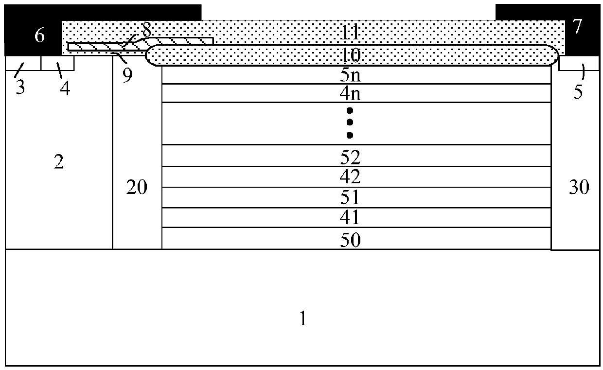
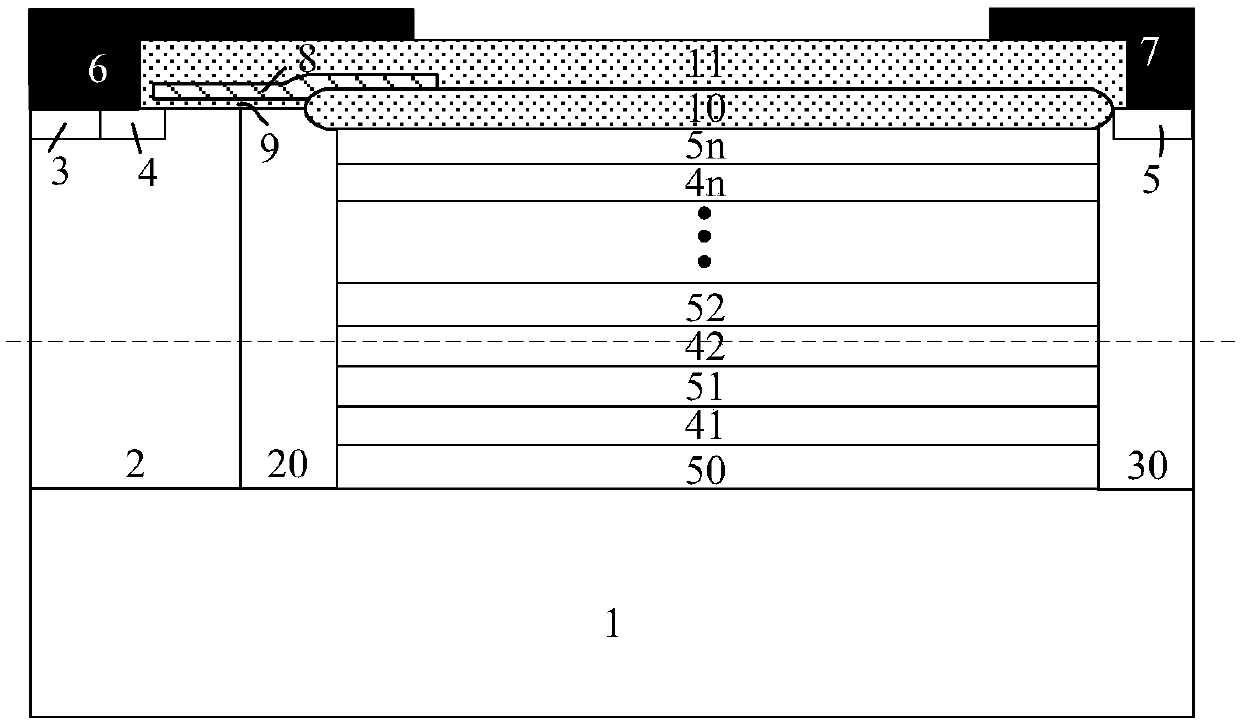
[0030] Such as figure 1As shown, an embodiment 1 of a lateral high voltage device, its cellular structure includes: a second conductivity type semiconductor substrate 1, a second conductivity type semiconductor 2 disposed on the upper end surface of the second conductivity type semiconductor substrate 1, disposed on The first conductivity type semiconductor drift region 50 on the upper end surface of the second conductivity type semiconductor substrate 1, the first conductivity type semiconductor drift region 50 is provided with stacked PN bars, and the PN bars include: disposed in the first conductivity type semiconductor drift region 50 The first layer of the second conductivity type buried layer 41, the first layer of the first conductivity type semiconductor 51 disposed on the upper surface of the first layer of the second conductivity type buried layer 41 in the first conductivity type semiconductor drift region 50, the first layer of the first conductivity type semiconduc...

Embodiment 2

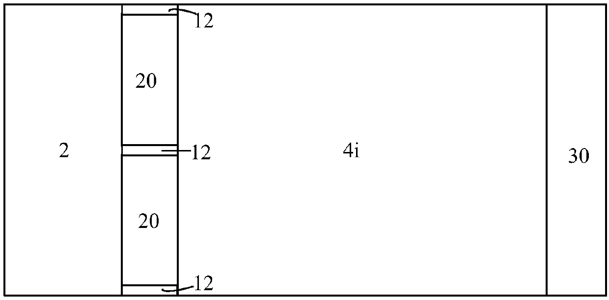
[0039] Such as image 3 As shown, the difference between this example and Example 1 is that the source first-conductivity-type JFET implantation region 20 uses multiple implants to finally form a stacked structure of multiple JFET implantation regions, including the source first-layer first-conductivity-type JFET Injection region 21, source second layer first conductivity type JFET injection 22... source first mth layer first conductivity type JFET injection region 2m, m≥1; drain first conductivity type JFET injection region 30 adopts multiple injections to finally Form a stacked structure of multiple JFET implantation regions, including the first drain layer first conductivity type JFET implantation region 31, the drain second layer first conductivity type JFET implantation 32...the drain mth layer first conductivity type JFET implantation region 3m, m≥1.

[0040] In this embodiment, the concentration distribution of the JFET region in the first embodiment is further optimiz...

Embodiment 3

[0042] Such as Figure 4 and Figure 5 As shown, the difference between this example and Example 2 is that neither the source first conductivity type JFET injection region 20 nor the drain first conductivity type JFET injection region 30 in this example is placed on the semiconductor surface, and the drift region is close to the source The end surface and the surface close to the drain end are all low-concentration first conductivity type semiconductor drift regions 50, and the lower end surface is not limited, and can be as follows Figure 4 The lower surfaces of the first JFET implantation region 21 of the first conductivity type of the source electrode and the JFET implantation region 30 of the first conductivity type of the drain electrode are all in contact with the semiconductor substrate 1 of the second conductivity type. Figure 5 The lower surfaces of the source first layer JFET implantation region 21 of the first conductivity type and the drain first conductivity ty...


PUM


Abstract

The invention provides a lateral high-voltage device. The cellular structure comprises a second conductive type semiconductor substrate, a second conductive type semiconductor and a first conductive type semiconductor drift region, wherein the first conductive type semiconductor drift region is provided with stacked PN strips, wherein each PN strip comprises a first layer of second conductive typeburied layer, a first layer of first conductive type semiconductor, a second layer of second conductive type semiconductor, a second layer of first conductive type semiconductor, the nth layer of second conductive type semiconductor and the nth layer of the first conductive type semiconductor; a source electrode first conductive type JFET injection region is arranged between the second conductivetype semiconductor and the stacked PN strips and located above the second conductive type semiconductor substrate; and a drain electrode first conductive type JFET injection region is arranged on theright side of the stacked PN strips and located above the second conductive type semiconductor substrate. The influence of depletion and even clamping of the JFET region to an unsaturated region of the device under the opening state of the device is effectively relieved, and an unsaturated region current of the device is improved.

Description

technical field [0001] The invention relates to the technical field of semiconductor power devices, in particular to a lateral high voltage device. Background technique [0002] Lateral high-voltage devices are an essential part of the development of high-voltage power integrated circuits. High-voltage power devices require high breakdown voltage, low on-resistance and low switching loss. To achieve a high breakdown voltage of a lateral high voltage device, the drift region used to withstand the voltage is required to have a long size and low doping concentration, but in order to meet the low on-resistance of the device, the drift region as a current channel is required to have a high doping concentration. In the design of power LDMOS (Latral Double-diffusedMOSFET) devices, breakdown voltage (Breakdown Voltage, BV) and specific on-resistance (Specific on-resistance, R on,sp ) has a contradictory relationship. When the device is used in high-voltage applications, the on-re...

Claims


Application Information

Patent Timeline
IPC IPC(8): H01L29/78H01L29/06
CPCH01L29/0615H01L29/0684H01L29/7816
Inventor 乔明叶力朱旭晗李珂林祺张波
Owner UNIV OF ELECTRONICS SCI & TECH OF CHINA
Why Eureka
Try Eureka