Superjunction device structure and preparation method thereof

A technology of super junction device and column structure, applied in the field of super junction device structure and its preparation, can solve the problem of uneven defect in super junction drift region, achieve optimized reverse recovery characteristics, reduce carrier life, and low cost Effect

Inactive Publication Date: 2019-09-06
上海功成半导体科技有限公司
View PDF7 Cites 1 Cited by
  • Summary
  • Abstract
  • Description
  • Claims
  • Application Information

AI Technical Summary

Problems solved by technology

[0005] In view of the above-mentioned shortcomings of the prior art, the object of the present invention is to provide a super junction device structure and its preparation method, which is used to solve the problem of uneven introduction of defects in the super junction drift region in the prior art

Method used


Image

  • Superjunction device structure and preparation method thereof
  • Superjunction device structure and preparation method thereof
  • Superjunction device structure and preparation method thereof

Examples


Embodiment 1

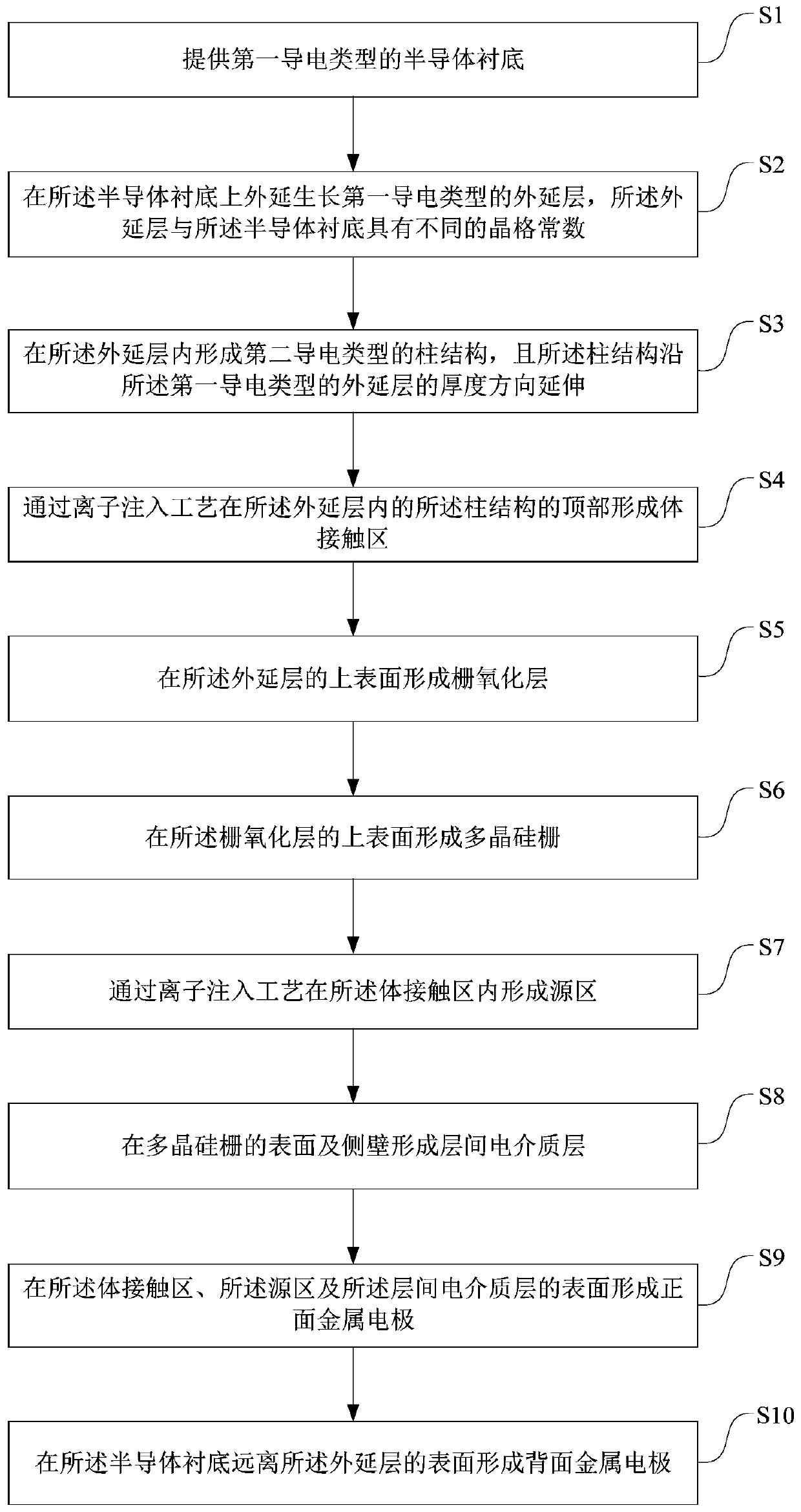
[0078] see Figure 1 to Figure 12 , the invention provides a method for preparing a superjunction device structure, comprising the following steps:

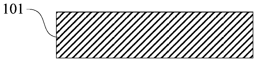
[0079] 1) providing a semiconductor substrate 101 of the first conductivity type;

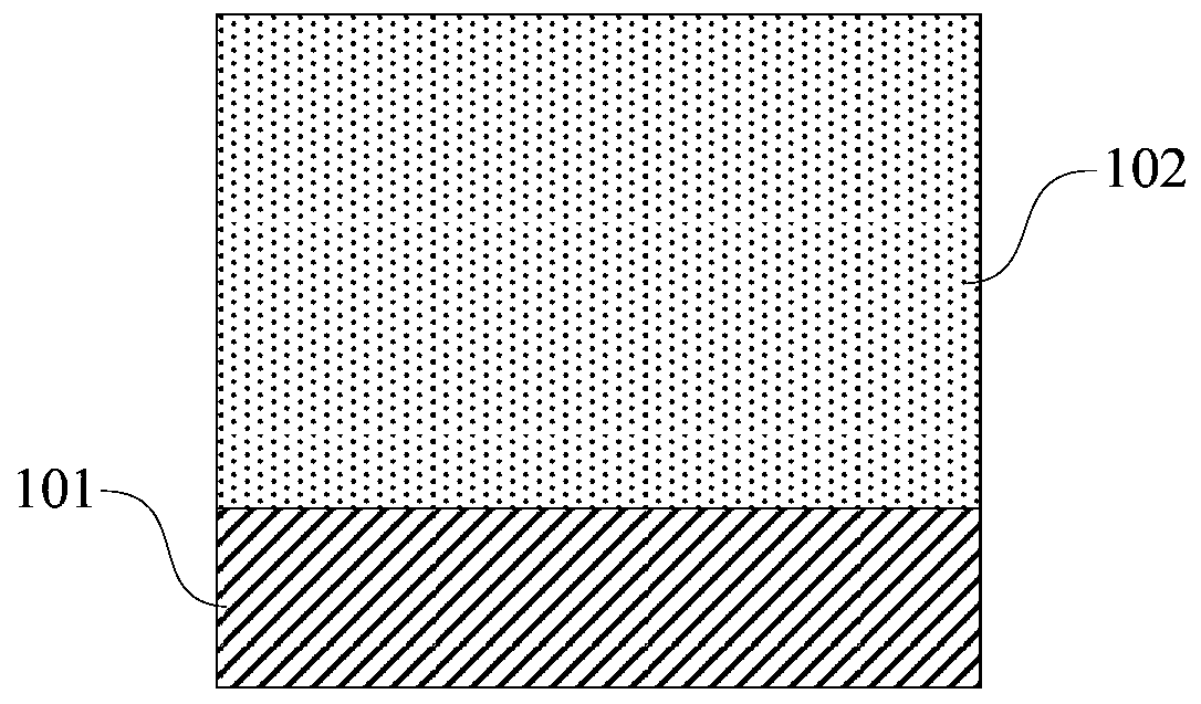
[0080] 2) epitaxially growing an epitaxial layer 102 of the first conductivity type on the semiconductor substrate 101, the epitaxial layer 102 having a different lattice constant from the semiconductor substrate 101;

[0081] 3) Forming a column structure 103 of the second conductivity type in the epitaxial layer 102 , and the column structure 103 extends along the thickness direction of the epitaxial layer 102 .

[0082] In step 1), see figure 1 The S1 step and figure 2 , providing a semiconductor substrate 101 of the first conductivity type. figure 2 is a schematic cross-sectional view of the semiconductor substrate 101. Optionally, in this embodiment, the first conductivity type is n-type, and the semiconductor substrate 101 is an n-typ...

Embodiment 2

[0121] see Figure 13 , this embodiment provides a super junction device structure and its preparation method. Compared with Embodiment 1, the difference of this embodiment is that the constituent material of the column structure 203 is germanium silicon material, and through the 103 a is epitaxially filled with silicon germanium material to form the column structure 203 .

[0122] As an example, in Figure 13 Among them, the super junction device structure includes a semiconductor substrate 201 of the first conductivity type, an epitaxial layer 202 of the first conductivity type and a column structure 203 of the second conductivity type, wherein the material of the column structure 203 is silicon germanium Material. Such as Figure 13 As shown, the super junction device structure further includes: a body contact region 204 , a gate oxide layer 205 , a polysilicon gate 206 , a source region 207 , an interlayer dielectric layer 208 , a front metal electrode 209 and a back me...


PUM


Abstract

The invention provides a superjunction device structure and a preparation method thereof. The superjunction device structure comprises a first conducting type semiconductor substrate; a first conducting type epitaxial layer arranged on the upper surface of the semiconductor substrate, wherein the epitaxial layer and the semiconductor substrate have different lattice constants; and a second conducting type column structure, which is arranged in the epitaxial layer and extends in the thickness direction of the epitaxial layer. By growing the epitaxial layer with different lattice constants fromthe semiconductor substrates, and introducing uniform controllable defects, probability of carrier recombination is increased and carrier life is reduced to optimize the reverse recovery characteristic of the superjunction power device and realize the purpose of rapid reduction of carriers at the turn-off stage of the device; and the preparation method is simple in preparation process, low in costand suitable for large-scale manufacture.

Description

technical field [0001] The invention relates to the field of semiconductor integrated circuit manufacturing, in particular to a superjunction device structure and a preparation method thereof. Background technique [0002] Electric energy is closely related to our life, and the efficient utilization of electric energy is an important research topic in power electronics technology. Power devices are the core of power electronics technology and play an increasingly important role in our daily life. Power devices are mainly used as switching power supplies in power electronics technology. An ideal switch should have extremely high voltage withstand capability and excellent conductivity, as well as fast turn-off characteristics. In the 1990s, with the emergence of super-junction technology, the limitations of traditional silicon-based high-voltage devices were broken, and while achieving high withstand voltage, they had excellent conduction characteristics. [0003] At presen...

Claims


Application Information

Patent Timeline
Patent Type & Authority Applications(China)
IPC IPC(8): H01L29/78H01L29/06H01L21/336
CPCH01L29/66712H01L29/7802H01L29/0634
Inventor 徐大朋梁欢黄肖艳薛忠营罗杰馨柴展
Owner 上海功成半导体科技有限公司
Why Eureka
Try Eureka