Eureka AIR delivers breakthrough ideas for toughest innovation challenges, trusted by R&D personnel around the world.

Epitaxial structure of near-infrared VCSEL laser and manufacturing method thereof

An epitaxial structure and laser technology, applied in lasers, laser parts, semiconductor lasers, etc., can solve the problem that it is difficult to meet the application requirements of near-infrared sensors, the design of the MQW structure in the active region is unreasonable, and the carrier gain in the active region is not large enough. and other problems, to achieve the effect of reducing leakage loss, increasing differential gain, and increasing recombination probability

Inactive Publication Date: 2017-08-25
张永
View PDF0 Cites 10 Cited by
  • Summary
  • Abstract
  • Description
  • Claims
  • Application Information

AI Technical Summary

Problems solved by technology

[0005] The disadvantage of using this process is that the optical power of VCSEL is relatively small, and it is difficult to meet the application requirements of most near-infrared sensors.
The reason for the above defects is that the above method is that the carrier gain in the active area is not large enough, which may be caused by the growth quality of the material in the active area, or may be caused by the unreasonable design of the MQW structure in the active area.

Method used


Image

  • Epitaxial structure of near-infrared VCSEL laser and manufacturing method thereof
  • Epitaxial structure of near-infrared VCSEL laser and manufacturing method thereof
  • Epitaxial structure of near-infrared VCSEL laser and manufacturing method thereof

Examples


Embodiment 2

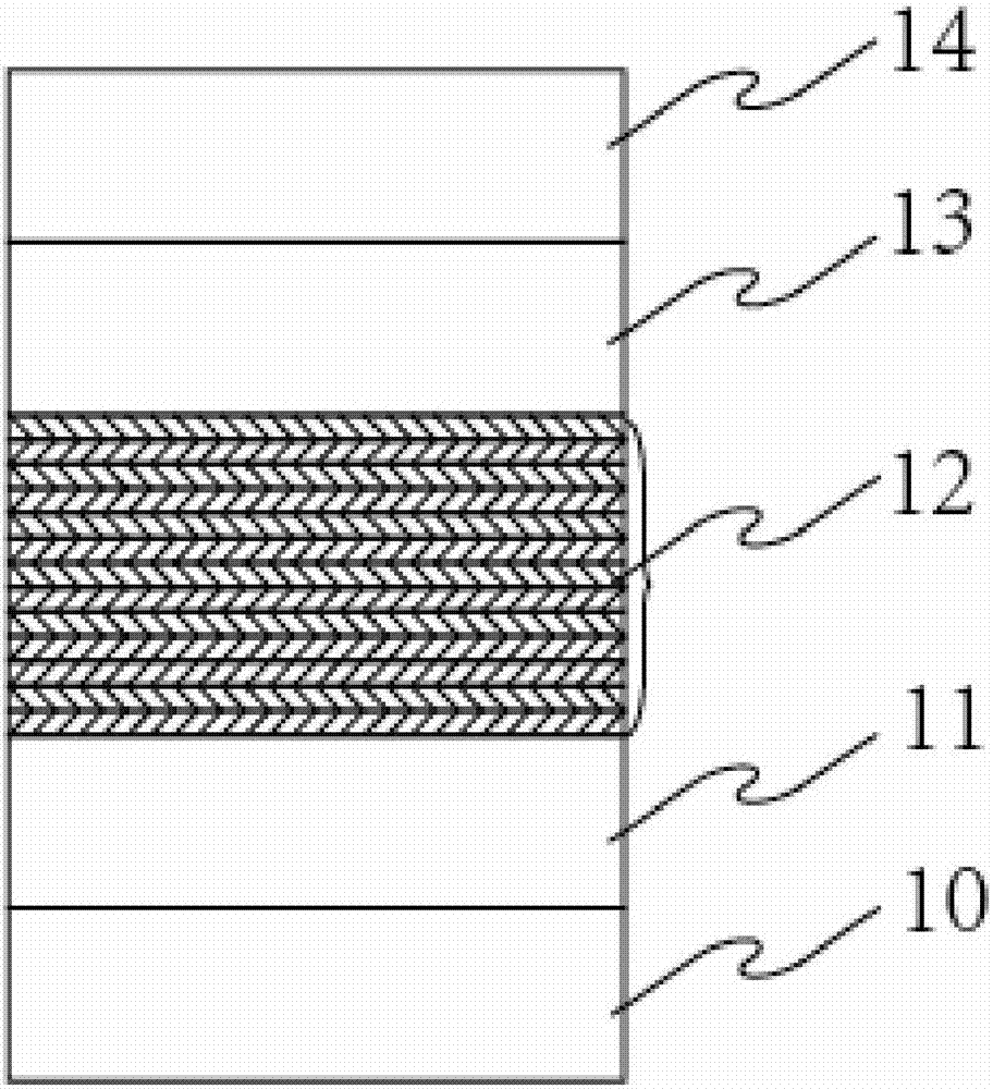
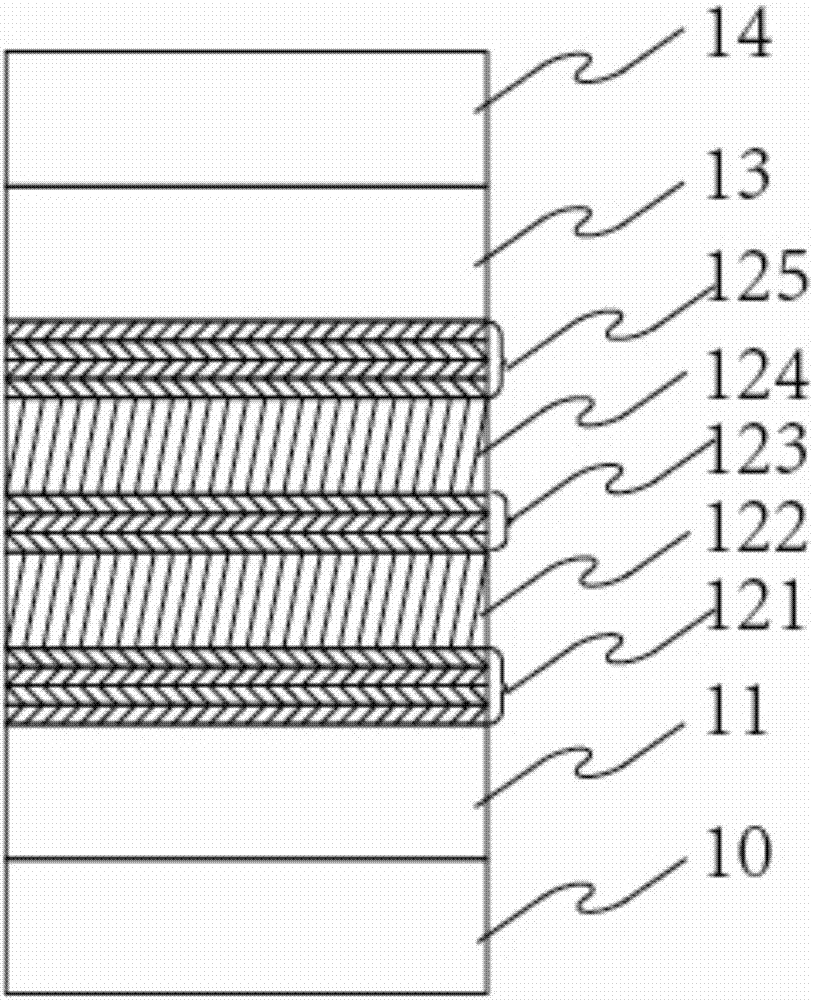
[0036] Such as Figure 4 As shown, the difference between the structure of this embodiment and the first embodiment lies in the structural design of the active region 12, and the active region of this embodiment is composed of the following epitaxial layers:

[0037] Layer 10: 45nm Al 0.90 Ga 0.10 As restriction layer;

[0038] Layer 11: 30nm Al 0.60 Ga 0.40 As to Al 0.10 Ga 0.90 A waveguide layer with a graded As composition;

[0039] Layer 12: Multiple Groups by In 0.12 Ga 0.88 As well and Al 0.10 Ga 0.90 Quantum wells composed of As barriers;

[0040] In the structure of the present invention, the quantum well 12 includes a first quantum well layer 1210, a first thick barrier layer 1220, a second quantum well layer 1230, a second thick barrier layer 1240 and a third quantum well layer 1250, the first quantum well Layer 1210 includes 3nmIn 0.12 Ga 0.88 As well, 6nm Al 0.10 Ga 0.90 As barrier, 3nmIn 0.12 Ga 0.88 As well, the first thick barrier layer 1220 in...


PUM


Abstract

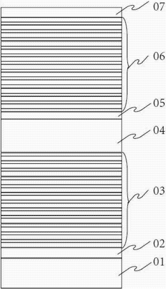
The invention provides an epitaxial structure of a near-infrared VCSEL laser. The structure comprises a GaAs substrate. A GaAs buffer layer, an N-type doped DBR, an active layer, an oxidation limiting layer, a P-type doped DBR and an ohmic contact layer are successively deposited on the GaAs substrate. The active layer successively comprises a limiting layer, a waveguide layer, a quantum well, a symmetrical waveguide layer and a symmetrical limiting layer. The quantum well is formed by multiple groups of quantum well layers. A thick barrier layer is arranged between the two adjacent groups of quantum well layers. A thickness of the thick barrier layer is greater than 50nm. In the epitaxial structure of the near-infrared VCSEL laser, through inserting the plurality of thick barrier layers in an active area quantum well, leakage losses of a carrier are reduced, a compound probability of an active area carrier is increased, a differential gain of the active area is improved and radiation power of the VCSEL laser is increased. Simultaneously, a limiting factor of active area photon is increased and a response rate of the VCSEL laser is improved.

Description

technical field [0001] The invention relates to a near-infrared VCSEL laser, in particular to an epitaxial structure and a preparation method of the near-infrared VCSEL laser. Background technique [0002] The vertical cavity surface emitting laser (VCSEL) forms a resonant cavity through a Bragg reflector (DBR), and the light is emitted from the direction perpendicular to the surface of the semiconductor substrate. Compared with edge-emitting semiconductor lasers, VCSEL has no optical cavity surface damage, has low threshold current, dynamic single-mode operation, small far-field divergence angle, near-circular spot and light direction perpendicular to the substrate surface, and has the characteristics of optical fiber coupling efficiency. High, easy to integrate two-dimensional array, so VCSEL has a wide range of applications in optical interconnection, optical communication, optical signal processing, WDM optical fiber communication, neural network, and computer chips. Ba...

Claims


Application Information

Patent Timeline
Patent Type & Authority Applications(China)
IPC IPC(8): H01S5/34H01S5/183H01S5/32
CPCH01S5/34H01S5/18305H01S5/32
Inventor 张永
Owner 张永
Why Eureka
Eureka Blog
Learn More