High-order surface grating surface-emitting semiconductor laser

A surface grating and laser technology, applied in the field of optical communication devices, can solve the problems of limited grating etching depth, short grating period, unfavorable laser output power, etc., and achieve the effects of reduced manufacturing difficulty and requirements, low cost and high manufacturing efficiency

Active Publication Date: 2017-06-13
HUAZHONG UNIV OF SCI & TECH
View PDF5 Cites 11 Cited by
  • Summary
  • Abstract
  • Description
  • Claims
  • Application Information

AI Technical Summary

Problems solved by technology

[0004] Aiming at the defects of the prior art, the object of the present invention is to provide a high-order surface grating surface-emitting semiconductor laser, which aims to solve the problem that the grating-cou

Method used


Image

  • High-order surface grating surface-emitting semiconductor laser
  • High-order surface grating surface-emitting semiconductor laser
  • High-order surface grating surface-emitting semiconductor laser

Examples


Embodiment Construction

[0021] In order to make the object, technical solution and advantages of the present invention clearer, the present invention will be further described in detail below in conjunction with the accompanying drawings and embodiments. It should be understood that the specific embodiments described here are only used to explain the present invention, not to limit the present invention.

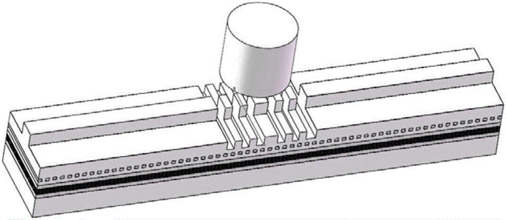
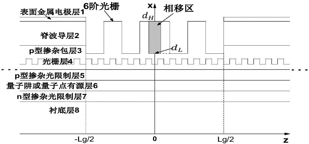
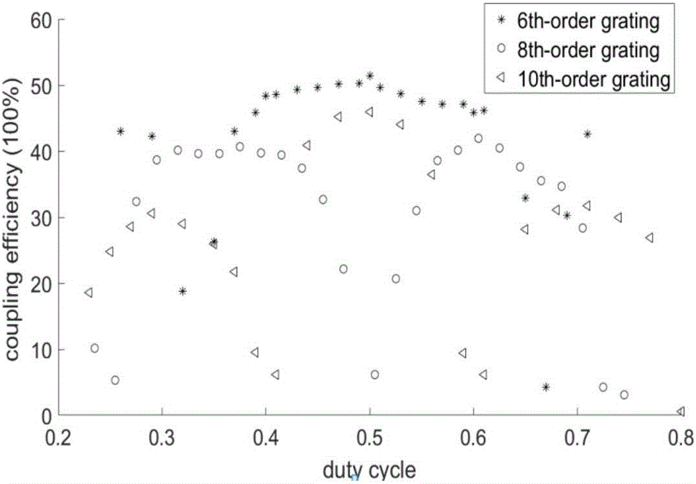
[0022] The invention belongs to the technical field of surface emitting distributed feedback semiconductor laser (SE-DFB). The invention solves the disadvantages that the existing grating-coupled surface-emitting semiconductor lasers are difficult to manufacture due to the design and are unfavorable for large-scale industrial production. Existing grating-coupled surface-emitting lasers generally use second-order gratings. The second-order grating corresponding to the 1.55-micron communication band has a grating period usually less than 500nm, which causes the existing grating-coupled surface-emitt...


PUM

PropertyMeasurementUnit
Lengthaaaaaaaaaa
Depthaaaaaaaaaa
Cycleaaaaaaaaaa

Abstract

The invention discloses a high-order surface grating surface-emitting semiconductor laser. The laser comprises a surface metal electrode layer, a ridge waveguide layer, a p-type doped cladding layer, a grating layer, a p-type doped optical confinement layer, a quantum well or quantum dot active area, an n-type doped optical confinement layer and a substrate layer, which are sequentially arranged, wherein a first-order grating is distributed on the grating layer; a high-order surface grating for coupling optical energy resonating along the horizontal direction to the perpendicular direction for output is distributed above the first-order grating in the center of a resonant cavity. The length of the high-order surface grating positioned above the grating layer in the center of the resonant cavity of the laser is (9 to 100) microns. A traveling wave mode in the resonant cavity of the laser is coupled into a radiation mode to realize surface output of laser by the high-order surface grating. The surface output light of the laser is directly coupled with a fiber core of a standard single-mode optical fiber. A segment of central phase shift is introduced into the center of the high-order surface grating, so that the coupling efficiency of the high-order surface grating surface-emitting laser and the standard single-mode optical fiber can exceed 50 percent.

Description

technical field [0001] The invention belongs to the technical field of optical communication devices, and more specifically relates to a high-order surface grating surface-emitting semiconductor laser. Background technique [0002] Semiconductor lasers are commonly used in optical transceivers for telecommunications and data communication networks. The lasers commonly used in the field of optical communication are edge-emitting lasers. The edge-emitting laser means that the light emitting direction of the laser is parallel to the active layer (a characteristic layer of the semiconductor laser), that is, in the horizontal direction, the light is emitted from the end face. The beam divergence angle of the edge-emitting laser is large, the spot is usually elliptical, and the coupling efficiency with the fiber is low. It usually requires a lens or other discrete optical components to be coupled to the fiber, and it needs to be cleaved into bars during testing, which results in ...

Claims


Application Information

Patent Timeline
IPC IPC(8): H01S5/18H01S5/12
CPCH01S5/1228H01S5/18
Inventor 张敏明敖应权刘德明
Owner HUAZHONG UNIV OF SCI & TECH
Why Eureka
Try Eureka