

Tunable, superconducting, surface-emitting teraherz source
- Summary
- Abstract
- Description
- Claims
- Application Information
AI Technical Summary
Benefits of technology
Problems solved by technology
Method used
Image

Examples
Embodiment Construction
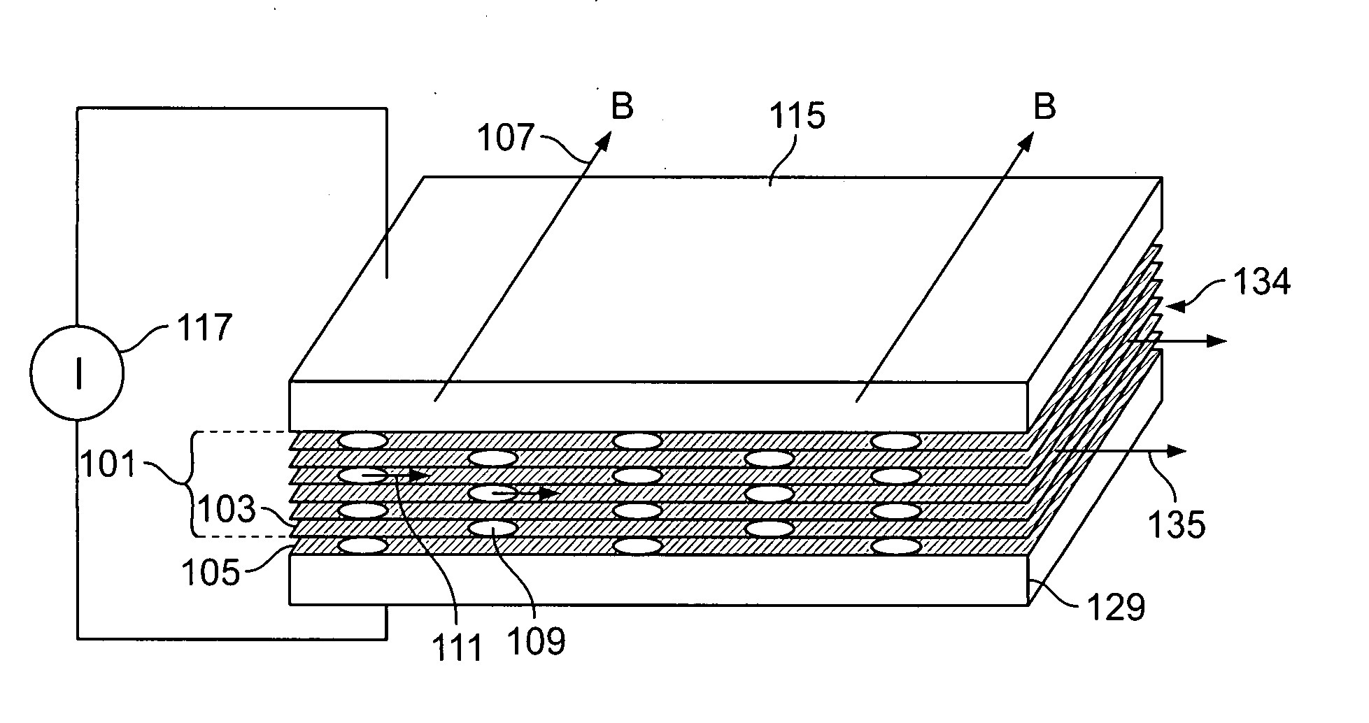
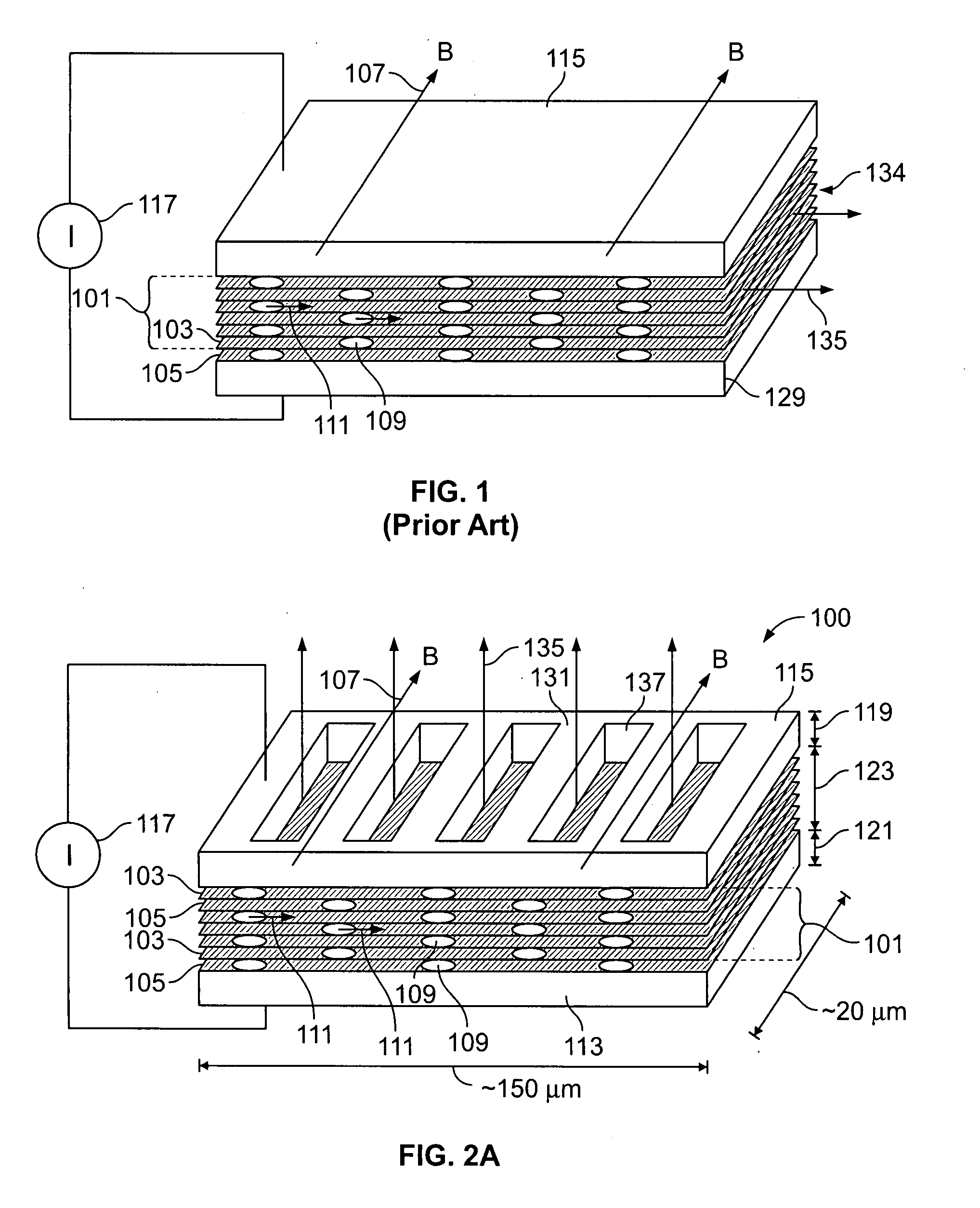
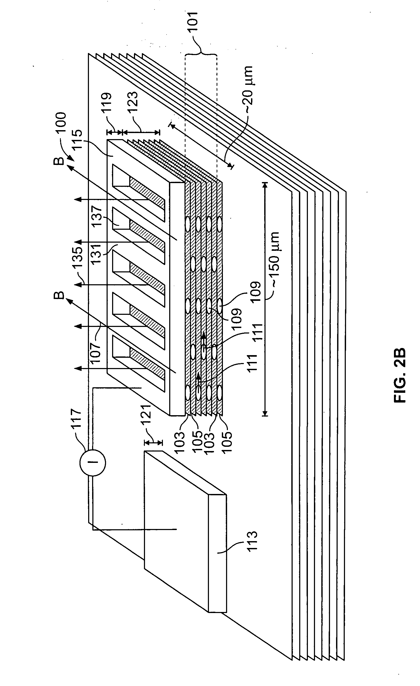
[0011] In accordance with an embodiment of the invention, a THz emitter includes a stack 101 of superconducting layers 103 that are separated by insulating layers 105 (see FIGS. 2A and 2B). In FIG. 2A these layers 103, 105 are disposed between a top metal layer 115 and a bottom metal layer 113, generally gold, a gold alloy or any conventional accepted conductor layer. As shown in FIGS. 2A and 2B, the entire device 100 is quite thin, with the top metal layer 115 having a thickness denoted as 119 and the bottom layer 113 having a thickness denoted as 121. In one preferred embodiment, each of the top and bottom layers 115, 121 have a thickness of about 75 nm each. The superconducting stack 101 has a thickness labeled as 123 (see FIG. 2A), and in one preferred embodiment the superconducting stack 101 thickness is less than about 100 nm. The thickness denoted 123 comprises a series of the superconducting layers 103 separated by insulating layer portions 105. In FIG. 2A electrical contact...
PUM
 Abstract
Description
Claims
Application Information