Manufacturing method of epitaxial wafer of GaN-based light emitting diode

A technology of light-emitting diodes and epitaxial wafers, which is applied in the direction of electrical components, circuits, semiconductor devices, etc., and can solve the problems of low luminous efficiency of GaN-based light-emitting diodes

Inactive Publication Date: 2014-07-02
HC SEMITEK SUZHOU
View PDF3 Cites 9 Cited by
  • Summary
  • Abstract
  • Description
  • Claims
  • Application Information

AI Technical Summary

Problems solved by technology

[0006] In order to solve the problem of low luminous efficiency of GaN-based light-emitting diodes caused by the strong piezoelectric polarization electric field effect of t

Method used


Image

  • Manufacturing method of epitaxial wafer of GaN-based light emitting diode
  • Manufacturing method of epitaxial wafer of GaN-based light emitting diode
  • Manufacturing method of epitaxial wafer of GaN-based light emitting diode

Examples


Embodiment 1

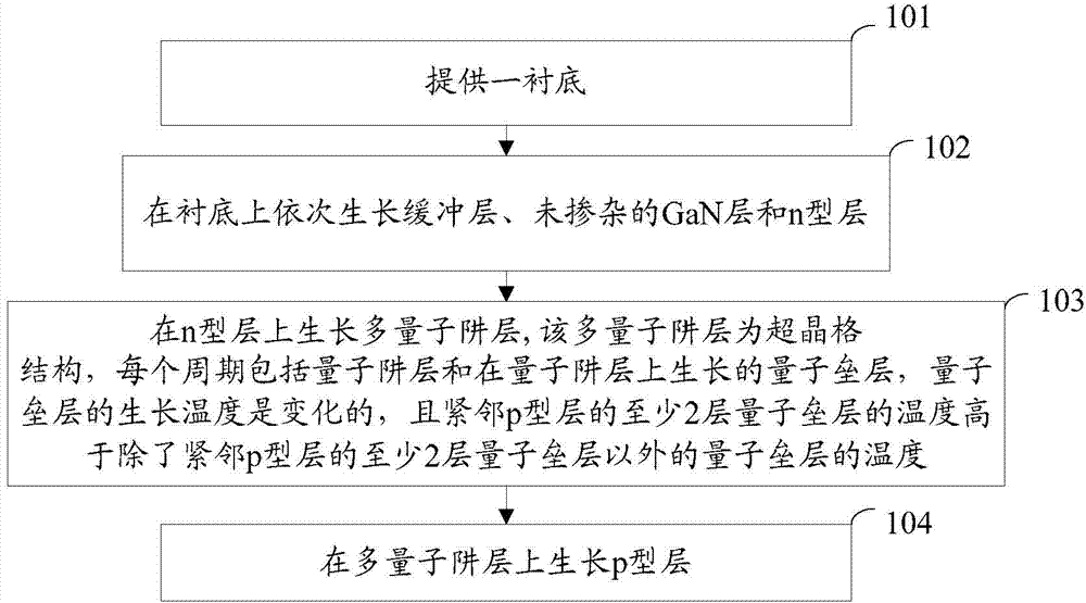
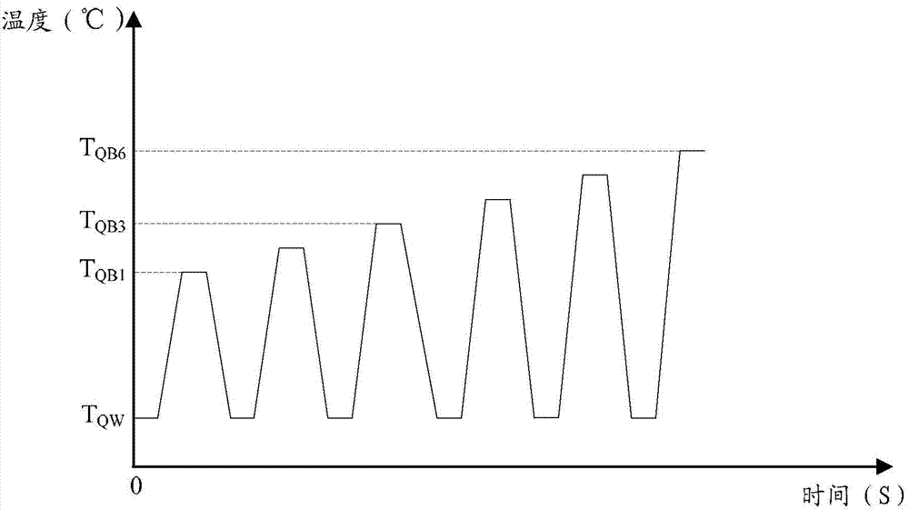
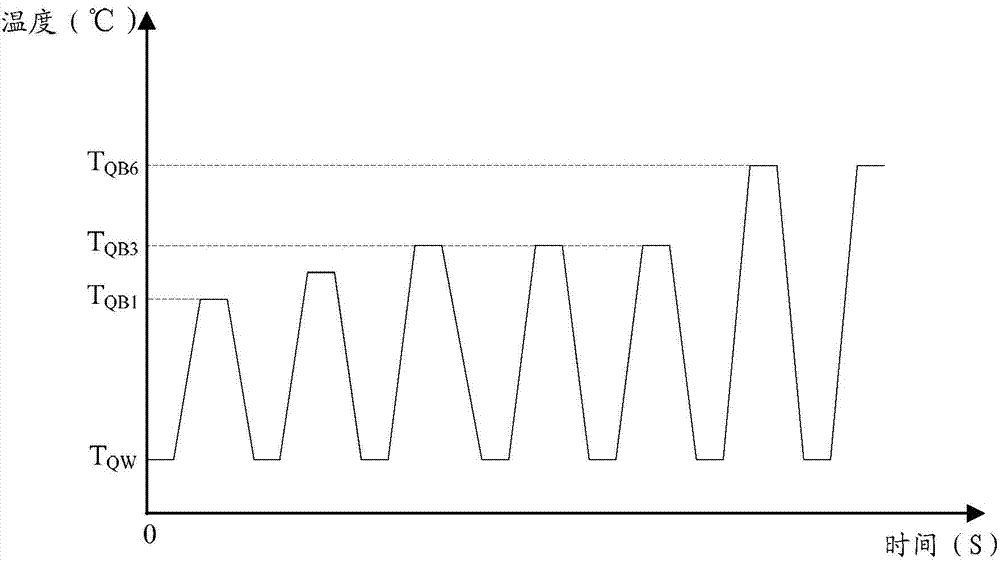
[0029] An embodiment of the present invention provides a method for preparing an epitaxial wafer of a GaN-based light-emitting diode, see figure 1 , the method includes:

[0030] Step 101: Provide a substrate.

[0031] The substrate includes, but is not limited to, a sapphire substrate.

[0032] When it is realized, the sapphire substrate can be heated to 1060°C in a MOCVD (Metal-organic Chemical Vapor Deposition) reaction chamber, and the sapphire substrate can be annealed and nitrided in a hydrogen atmosphere for 10 minutes. to clean the substrate surface.

[0033] Step 102: growing a buffer layer, an undoped GaN layer and an n-type layer sequentially on the substrate.

[0034] Wherein, the buffer layer may be a gallium nitride layer, an aluminum nitride layer, or an aluminum gallium nitride layer or the like.

[0035] The n-type layer may be a Si-doped GaN layer, but not limited to Si-doped. During implementation, silane can be selected to complete the silicon doping i...

Embodiment 2

[0060] An embodiment of the present invention provides a method for preparing an epitaxial wafer of a GaN-based light-emitting diode. The method for preparing the epitaxial wafer in this embodiment is basically the same as that of Embodiment 1, except that the quantum barrier layer next to the p-type layer is The growth thickness is smaller than that of the quantum barrier layers other than the quantum barrier layer immediately adjacent to the p-type layer.

[0061] Specifically, starting from the side of the n-type layer, the growth thickness of all the quantum barrier layers in the multi-quantum well layer is gradually reduced, or the growth thickness of all the quantum barrier layers is kept constant and then gradually reduced.

[0062] When implemented, the growth thickness of the quantum barrier layer can be controlled by changing the growth time or growth rate of the quantum barrier layer. Specifically, the growth thickness of the quantum barrier layer is proportional to...


PUM

PropertyMeasurementUnit
Growth temperatureaaaaaaaaaa
Thicknessaaaaaaaaaa

Abstract

The invention discloses a manufacturing method of an epitaxial wafer of a GaN-based light emitting diode, and belongs to the technical field of semiconductors. The manufacturing method includes the steps that a substrate is provided; a buffer layer, an undoped GaN layer, an n-type layer, a multi-quantum well layer and a p-type layer are grown on the substrate in sequence, wherein the multiple quantum well layer is of a superlattice structure, each period includes a quantum well layer and a quantum barrier layer, and the growth temperature of at least two quantum barrier layers tightly adjacent to the p-type layer is higher than that of the quantum barrier layers except for the two quantum barrier layers. The growth temperature of the quantum barrier layers close to the n-type layer is low, crystal quality is poor, stress is relieved step by step, then the piezoelectric polarization effect is weakened, and growth of the quantum barrier layers close to the p-type layer is facilitated. As the growth temperature of the quantum barrier layers close to the p-type layer is high, the crystal quality is well improved, the full width at half maximum is decreased, the electron-hole composite probability is further improved, and then the light emitting efficiency of the GaN-based light emitting diode is improved.

Description

technical field [0001] The invention relates to the technical field of semiconductors, in particular to a method for preparing an epitaxial wafer of a GaN-based light-emitting diode. Background technique [0002] LED (Lighting Emitting Diode, light-emitting diode) is known as the most promising green lighting source in the 21st century because of its small size, low power consumption, long service life, high brightness, low heat, environmental protection, and durability. The GaN material series is an ideal short-wavelength light-emitting device material. The band gap of GaN and its alloys covers the spectral range from red to ultraviolet. At the same time, the GaN material series has low heat generation rate and high breakdown electric field, which is conducive to the operation of devices under high power conditions. Therefore, GaN material series are widely used in LEDs. [0003] The epitaxial wafer of the existing GaN-based light-emitting diode usually includes a substra...

Claims


Application Information

Patent Timeline
IPC IPC(8): H01L33/00
CPCH01L33/0075
Inventor 武艳萍魏世祯谢文明
Owner HC SEMITEK SUZHOU
Why Eureka
Try Eureka