An extremely low reverse recovery charge superjunction power vdmos

A technology of reverse recovery charge and power, applied in circuits, electrical components, electric solid-state devices, etc., can solve problems such as improving the reverse recovery characteristics of SJ-VDMOS body diodes, the level of limited freewheeling current, and the increase of leakage current , to achieve excellent reverse recovery characteristics, improve reverse recovery characteristics, and reduce the effect of Qrr

Active Publication Date: 2020-12-11
SOUTHEAST UNIV
View PDF4 Cites 0 Cited by
  • Summary
  • Abstract
  • Description
  • Claims
  • Application Information

AI Technical Summary

Problems solved by technology

But this scheme inevitably leads to two acute problems
First, the improvement of body diode reverse recovery characteristics of SJ-VDMOS and the level of leakage current have a trade-off relationship with the size of the Schottky diode area. For example, the larger the area, the more obvious the improvement effect of reverse recovery characteristics, but the leakage current Second, the current capability of the Schottky diode is not as good as that of the SJ-VDMOS body diode, so that when a high freewheeling current flows, the body diode still plays a leading role in the freewheeling, which greatly reduces the reverse recovery characteristics of this scheme. improvement
It can be seen from the above that the existing parallel Schottky scheme cannot greatly improve the reverse recovery characteristics of the SJ-VDMOS body diode on the basis of maintaining a low leakage current level, and this technical scheme is limited by the freewheeling current level, only Under the lower freewheeling current, it can play a very good reverse recovery improvement

Method used


Image

  • An extremely low reverse recovery charge superjunction power vdmos
  • An extremely low reverse recovery charge superjunction power vdmos
  • An extremely low reverse recovery charge superjunction power vdmos

Examples


Embodiment Construction

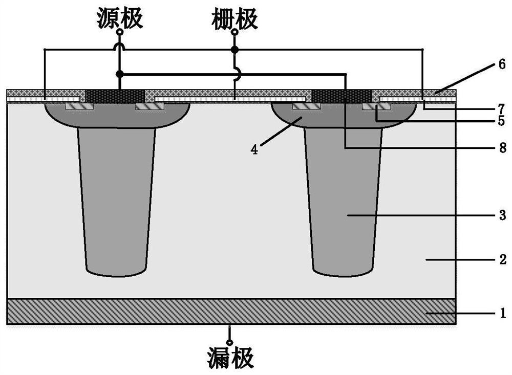
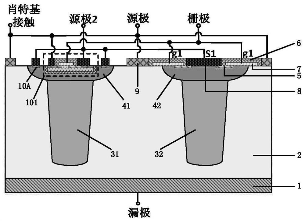
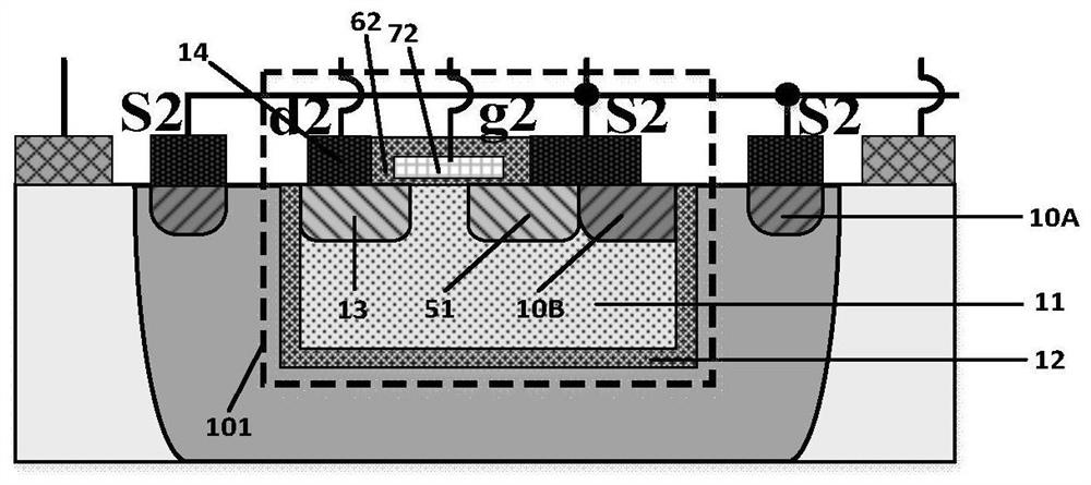
[0022] An extremely low reverse recovery charge superjunction power VDMOS, including a superjunction VDMOS, the superjunction VDMOS includes an N-type substrate 1 that doubles as a drain and an N-type drift region 2 disposed on the N-type substrate 1 , which is characterized in that a first P column 31 is provided in the N-type drift region 2 of the super junction VDMOS, and a first P-type body region 41 is provided on the top of the first P column 31, and the first P-type body region 41 The top surface is flush with the top surface of the N-type drift region 2, an N MOS transistor 101 is arranged on the first P-type body region 41, and an NMOS transistor 101 is arranged between the N MOS transistor 101 and the first P-type body region 41. With SiO 2 The isolation layer 12 is further provided with a first P-type heavily doped region 10A on the first P-type body region 41, the source metal of the super junction VDMOS, the source metal of the N MOS transistor 101 and the first P...


PUM

PropertyMeasurementUnit
depthaaaaaaaaaa
widthaaaaaaaaaa
lengthaaaaaaaaaa

Abstract

The present invention relates to a super-junction power VDMOS having an extremely low reverse recovery charge, comprising an N-type substrate also serving as a drain and an N-type drift region. A first P column is provided in the N-type drift region; a first P-type body region is provided in the top of the first P column; an NMOS is provided in the first P-type body region; a SiO2 isolation layer is provided between the NMOS and the first P-type body region; and a first P-type heavily doped region is provided in the first P-type body region. Source metal of a super-junction VDMOS, source metal of the NMOS, and the first P-type heavily doped region are connected; the drain of the super-junction VDMOS serves as the drain of the super-junction power VDMOS; the gate of the super-junction VDMOS and the gate of the NMOS are connected and serve as the gate of the super-junction power VDMOS; the drain of the NMOS serves as the source of the super-junction power VDMOS; and an N-type drift region of the super-junction VDMOS is provided with a Schottky contact which is connected to the drain of the NMOS, so as to form a Schottky diode of which the cathode and anode are respectively connected to the drain and source in the structure provided by the present invention.

Description

technical field [0001] The invention relates to the field of power semiconductor devices, in particular to a preparation method of a super junction power VDMOS device with extremely low reverse recovery charge Background technique [0002] Super Junction Vertical Double-diffusion Metal-oxide-semiconductor (SJ-VDMOS for short) breaks the limit of silicon, achieves extremely low on-resistance while maintaining high endurance of the device The voltage performance makes it widely used in pulse width modulation and motor control circuits. [0003] Traditional SJ-VDMOS introduces highly doped P-columns to deplete each other laterally with the high-concentration N-type withstand voltage layer to reduce the vertical electric field of the device and achieve high withstand voltage capability and low on-resistance of the device. However, the highly doped p-column greatly improves the anode emission area and hole injection efficiency of the SJ-VDMOS body diode, resulting in extremely p...

Claims


Application Information

Patent Timeline
Patent Type & Authority Patents(China)
IPC IPC(8): H01L29/06H01L29/78H01L27/06
CPCH01L27/06H01L29/06H01L29/78
Inventor 祝靖田甜李少红孙伟锋陆生礼时龙兴
Owner SOUTHEAST UNIV
Why Eureka
Try Eureka