Transistor with high performance, wide safety operation area and high reliability

A technology of safe working area and transistor, applied in wide safe working area, high-reliability transistor, high-performance field, can solve the problem of serious side effect of emitter current, increase the effective chip area, secondary Large breakdown withstand capacity, the effect of improving the current magnification

Inactive Publication Date: 2019-12-20
SHANDONG AOTIAN ELECTRONICS & TECH CO LTD
View PDF0 Cites 2 Cited by
  • Summary
  • Abstract
  • Description
  • Claims
  • Application Information

AI Technical Summary

Problems solved by technology

Therefore, at the collector-emitter voltage V CE When higher, the collector effect of the emitter current is more serious

Method used


Image

  • Transistor with high performance, wide safety operation area and high reliability
  • Transistor with high performance, wide safety operation area and high reliability
  • Transistor with high performance, wide safety operation area and high reliability

Examples


Embodiment 1

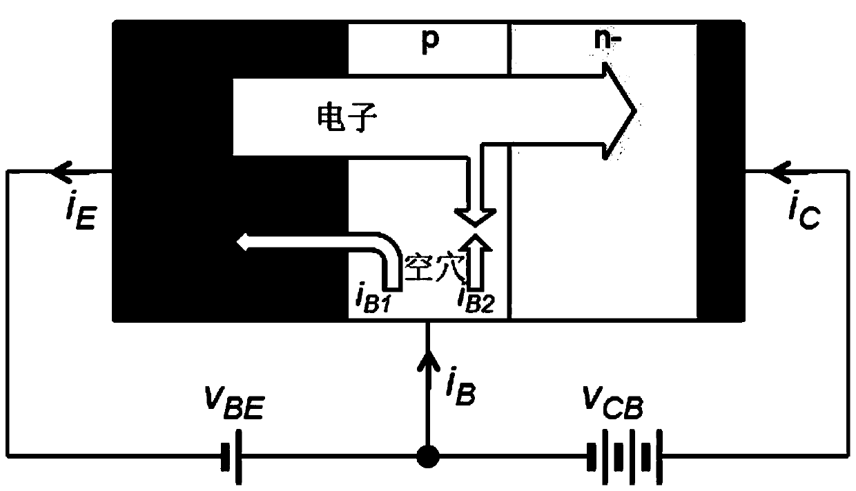
[0088] Embodiment 1, a transistor with high performance, wide safe working area, and high reliability includes several independent sub-transistors. The sub-transistors are formed by dividing the original large transistor as a whole. Transistors are separated electrically, that is, these sub-transistors are electrically separated and not connected to each other, but they are still a whole in physical form. The number of divided sub-transistors can be set according to performance requirements and production technology, ranging from tens to thousands; the division of the overall total current of the transistor is realized in each sub-transistor, so that the temperature of each part of the overall transistor is uniform, and the local current of the transistor is excessively increased are effectively suppressed.

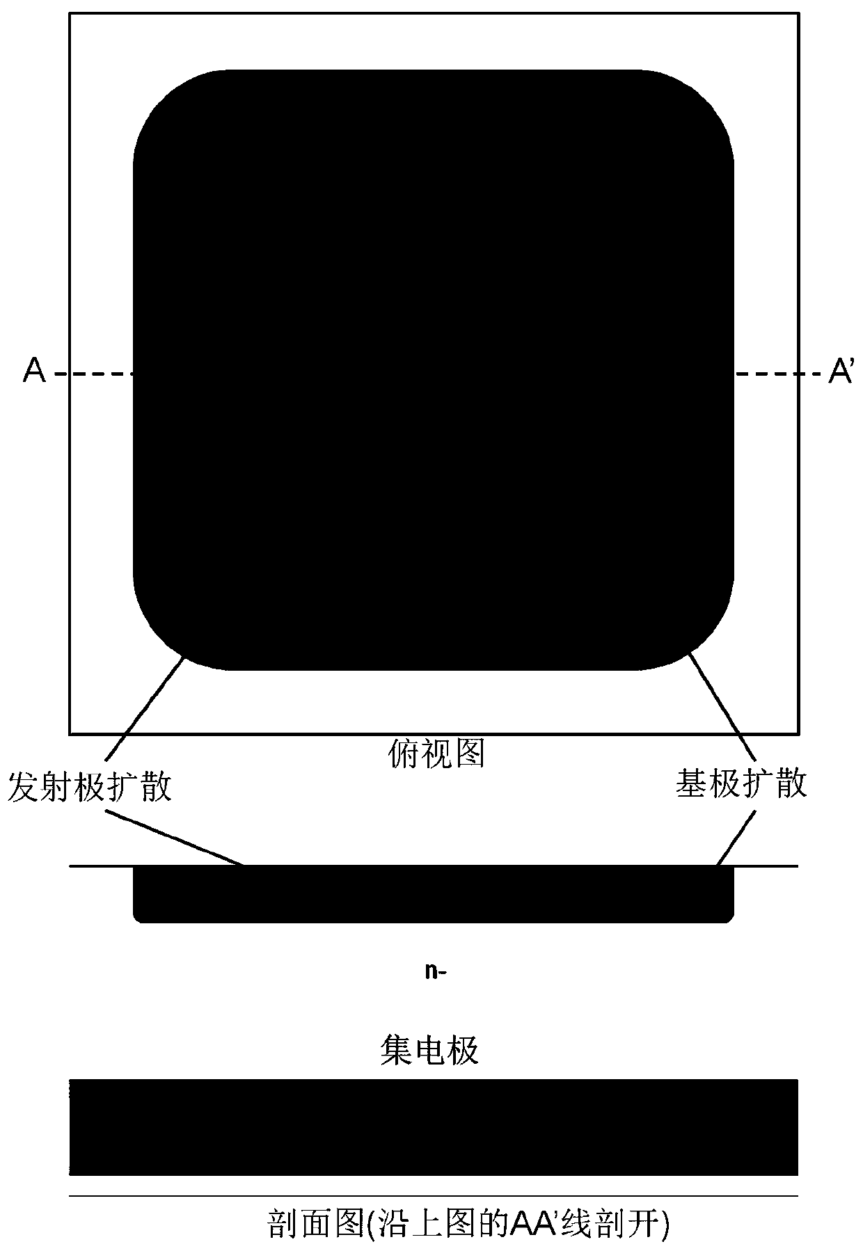
[0089] like image 3 As shown, the place marked by n- is the collector of the transistor, the place marked by p is the base of the transistor, the place marked by n+ is ...

Embodiment 2

[0100] Embodiment 2, a transistor with high performance, wide safe working area, and high reliability includes several sub-transistors independent of each other. Transistors are separated electrically, that is, these sub-transistors are electrically separated and not connected to each other, but they are still a whole in physical form. The number of divided sub-transistors can be set according to performance requirements and production technology, ranging from tens to thousands; the division of the overall total current of the transistor is realized in each sub-transistor, so that the temperature of each part of the overall transistor is uniform, and the local current of the transistor is excessively increased are effectively suppressed.

[0101] like image 3 As shown, the place marked by n- is the collector of the transistor, the place marked by p is the base of the transistor, the place marked by n+ is the emitter of the transistor, the base is the island in the collector,...

Embodiment 3

[0112]Embodiment 3, a transistor with high performance, wide safe working area, and high reliability includes several sub-transistors independent of each other. The sub-transistors are formed by dividing the original large transistor into several small Transistors are separated electrically, that is, these sub-transistors are electrically separated and not connected to each other, but they are still a whole in physical form. The number of divided sub-transistors can be set according to performance requirements and production technology, ranging from tens to thousands; the division of the overall total current of the transistor is realized in each sub-transistor, so that the temperature of each part of the overall transistor is uniform, and the local current of the transistor is excessively increased are effectively suppressed.

[0113] like image 3 As shown, the place marked by n- is the collector of the transistor, the place marked by p is the base of the transistor, the pl...


PUM


Abstract

The invention discloses a transistor with high performance, wide safety operation area and high reliability. The transistor comprises multiple mutually independent sub-transistors, and the sub-transistors are formed by entirely segmenting and spacing the original big transistor; the segmentation of the total current of the entire transistor is realized at each sub-transistor, so that the temperatures at multiple parts of the entire transistor are uniform, the excessive increasing of the local current of the transistor is effectively inhibited, and multiple sub-transistors are arranged on one monocrystalline silicon wafer. The transistor disclosed by the invention has the advantages of improving the secondary breakdown tolerance of the power transistor, broadening the safety operation arearange, reinforcing the reliability of the device and the electronic product, prolonging the service life of the transistor and the complete machine, and expanding the application field of the power transistor.

Description

technical field [0001] The high-performance, wide safe working area, and high-reliability crystal triode involved in the present invention are widely used in power amplifiers, ultrasonic generators, LED drivers, regulated power supplies, computers / tablet computers, flat-panel TVs / displays, instruments, meters, Motor drives, industrial power supplies, automobiles and other electronic equipment and applications. Background technique [0002] Transistor, also known as semiconductor triode, bipolar transistor, transistor, and triode, is a semiconductor device that uses base input current to control collector output current. [0003] Crystal transistors can amplify weak electrical signals into stronger electrical signals, and are widely used in low-frequency / high-frequency / radio frequency / microwave small signal and power amplifiers; voltage / constant current power supply, PWM motor drive, LED drive, and power control. [0004] The semiconductor material of the transistor may be ...

Claims


Application Information

Patent Timeline
Patent Type & Authority Applications(China)
IPC IPC(8): H01L29/732H01L27/02H01L27/082
CPCH01L27/0211H01L27/0823H01L29/732
Inventor 闫守礼
Owner SHANDONG AOTIAN ELECTRONICS & TECH CO LTD
Why Eureka
Try Eureka