Amplifier and class AB amplifier
A technology of amplifiers and transistors, applied in amplifiers, power amplifiers, improved amplifiers to improve efficiency, etc., can solve problems such as inability to fully amplify the full wave
- Summary
- Abstract
- Description
- Claims
- Application Information
AI Technical Summary
Problems solved by technology
Method used
Image
Examples
Embodiment Construction
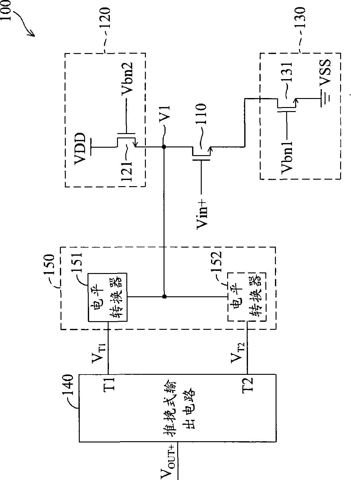
[0011] figure 1 It is a schematic diagram of an embodiment of the amplifier of the present invention. Such as figure 1 As shown, the amplifier 100 includes an input transistor 110, an impedance unit 120, a current source 130, a push-pull output circuit 140, and a level conversion unit 150.
[0012] The input transistor 110 receives the input voltage Vin+. In this embodiment, the input transistor 110 is an NMOS transistor, its gate receives the input voltage Vin+, its drain is coupled to the impedance unit 120 at a node, and its source is coupled to the current source 130. The voltage of the node is the voltage V1, where the voltage V1 is the intermediate voltage generated by the input transistor 110.
[0013] The impedance unit 120 is coupled to the input transistor 110. In this embodiment, the impedance unit 120 is an NMOS transistor 121. The gate of the NMOS transistor 121 receives the voltage Vbn2, the drain thereof receives the voltage VDD (such as the supply voltage), and ...
PUM
 Abstract
Description
Claims
Application Information


