Methods of patterning a material on polymeric substrates

A polymeric, patterned technology, applied in the use/removal method of circuit mask, photolithography/patterning, patterning and photolithography, etc., which can solve the problem of difficult tool repositioning

Inactive Publication Date: 2009-09-09
3M INNOVATIVE PROPERTIES CO
View PDF24 Cites 5 Cited by
  • Summary
  • Abstract
  • Description
  • Claims
  • Application Information

AI Technical Summary

Problems solved by technology

This value is 1000 times greater than the required 3 micron place

Method used


Image

  • Methods of patterning a material on polymeric substrates
  • Methods of patterning a material on polymeric substrates
  • Methods of patterning a material on polymeric substrates

Examples


example 1

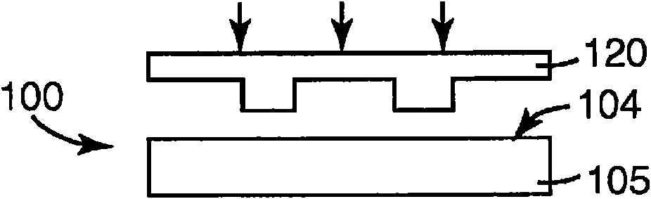
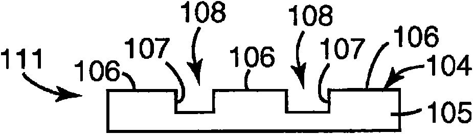
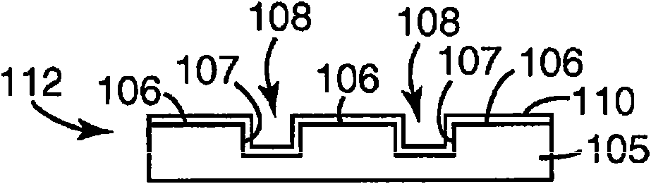
[0061] Substrate preparation

[0062] A 250 micron thick clear polycarbonate film (available under the tradename Lexan from the General Electric Company, Fairfield, CT) at the General Electric Plastics Division in Pittsfield, Massachusetts ( GE Plastics division, Pittsfield, MA)), heat embossed with a relief pattern of recessed grid lines (complementary to raised squares). The molded tool was fabricated from a circular fused silica plate with a diameter of 10 cm by photolithography and reactive ion etching. The tool included ridges 10 microns wide and approximately 10 microns high that defined gridlines of a square grid with a pitch of 200 microns. Molding was performed by pressing with a force of 10,000 Newtons using a Model AUTO M laminating press (available from Carver, Inc., Wabash, IN), Molding Tool The polycarbonate film was pressed at 176°C for 15 minutes. The embossed film included channels 10 microns wide and approximately 10 microns deep defining gridlines of a ...


PUM

PropertyMeasurementUnit
Heightaaaaaaaaaa
Widthaaaaaaaaaa
Thicknessaaaaaaaaaa

Abstract

A method of patterning a first material (110) on a polymeric substrate (105) is described. The method includes providing a polymeric film substrate (105) having a major surface (104) with a relief pattern including a recessed region (108) and an adjacent raised region (106), depositing a first material (110) onto the major surface (104) of the polymeric film substrate (105) to form a coated polymeric film substrate, forming a layer of a functionalizing material (131) selectively on the raised region (106) of the coated polymeric film substrate to form a functionallzed raised region and an unfunctionalized recessed region, and etching the first material (110) from the polymeric substrate selectively from the unfunctionalized recessed region.

Description

Background technique [0001] The present invention generally relates to methods of patterning materials on polymeric substrates and articles formed by such methods. [0002] Polymeric films with patterns of metallic materials have a variety of commercial applications. In some cases, it is desirable for the conductive grid to be thin enough to be invisible to the naked eye and supported on a transparent polymeric substrate. Transparent conductive sheets are used in a variety of applications including, for example, resistively heated windows, electromagnetic interference (EMI) shielding, static dissipating components, antennas, touch screens for computer monitors, and electrochromic windows, optoelectronic devices, electroluminescent devices and surface electrodes of liquid crystal displays. [0003] The use of substantially transparent conductive grids for such applications as EMI shielding is known. Grids can be made from a mesh or screen of wires sandwiched or laminated bet...

Claims


Application Information

Patent Timeline
IPC IPC(8): H05K3/00H05K3/06
CPCH05K2203/0108H05K1/0393H05B2203/017H05B3/84H05K9/0096H05K2201/09045H05K2203/0528H05K2201/09036H05K2203/0537H05K2203/1545H05K3/0014H05K3/061C23F1/02C23F1/14Y10T428/24479Y10T428/268H05K3/0079
Inventor 马修·H·弗雷庆·P·阮
Owner 3M INNOVATIVE PROPERTIES CO
Why Eureka
Try Eureka