Method of lithography patterning

A technology of graphics and lithography, applied in photography, photoengraving process of pattern surface, optics, etc., can solve the problems of inappropriateness and inconvenience of general process methods

Active Publication Date: 2012-05-30
TAIWAN SEMICON MFG CO LTD
View PDF4 Cites 0 Cited by
  • Summary
  • Abstract
  • Description
  • Claims
  • Application Information

AI Technical Summary

Problems solved by technology

[0003] It can be seen that the above-mentioned existing lithographic pattern forming technology obviously still has inconvenience and defects in the processing method and use, and needs to be further improved urgently.
In order to solve the above problems, the relevant manufacturers have tried their best to find a solution, but no suitable design has been developed for a long time, and there is no suitable method to solve the above problems in general process methods. This is obviously a problem. Issues that relevant industry players are eager to solve

Method used


Image

  • Method of lithography patterning
  • Method of lithography patterning
  • Method of lithography patterning

Examples


Embodiment Construction

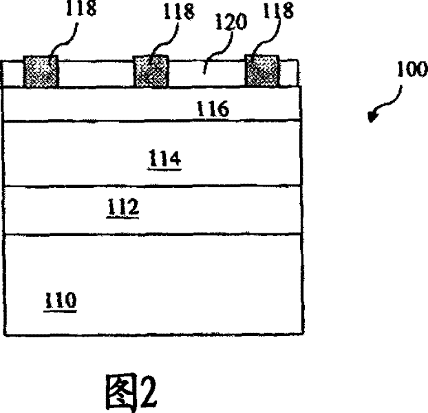
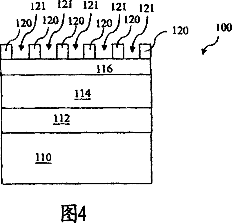
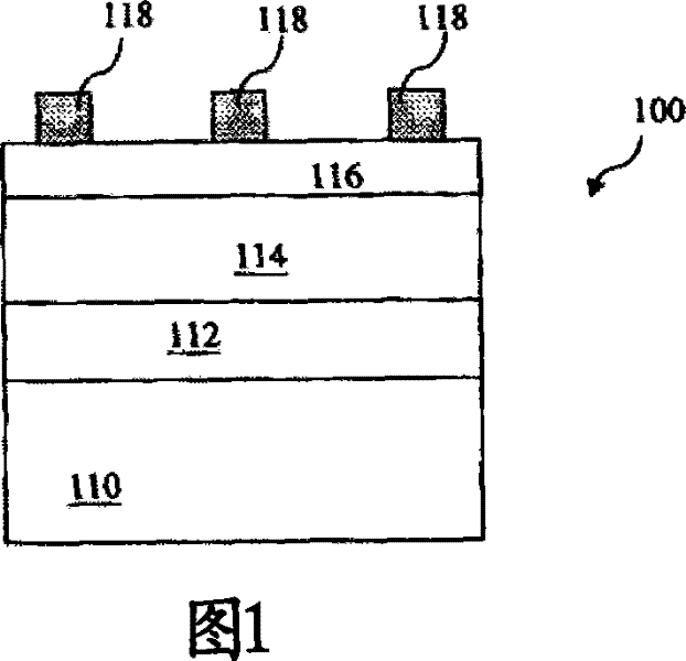
[0037] In order to further explain the technical means and effects that the present invention adopts to achieve the intended invention purpose, the specific implementation methods, steps, features and features of the lithography pattern forming method proposed according to the present invention will be described below in conjunction with the accompanying drawings and preferred embodiments. Efficacy, detailed as follows.

[0038] The following description discloses many different embodiments, revealing some special combinations and arrangements. However, these embodiments are only examples, and thus do not limit the scope of the present invention. for example. The description of forming a first object on a second object may include embodiments in which the first and second objects are formed in direct contact, and may also include embodiments in which other objects are formed between the first and second objects, therefore The first and second objects are not in direct contac...


PUM

PropertyMeasurementUnit
thicknessaaaaaaaaaa
thicknessaaaaaaaaaa
thicknessaaaaaaaaaa

Abstract

The invention relates to a method of lithography patterning includes forming a first resist pattern on a substrate, the first resist pattern including a plurality of openings therein on the substrate; forming a second resist pattern on the substrate and within the plurality of openings of the first resist pattern, the second resist pattern including at least one opening therein on the substrate; and removing the first resist pattern to uncover the substrate underlying the first resist pattern. The method of lithography patterning of the invention can reduce procudtion cost and reduce effection of critical dimension variation.

Description

technical field [0001] The invention relates to a lithographic pattern forming method, in particular to a lithographic pattern forming method for forming contact holes and grooves. Background technique [0002] Semiconductor technology continues to move toward smaller dimensions in modern times. In recent years, the size has evolved to 65nm, 45nm, and even smaller processes (processes are manufacturing processes, which are referred to herein as processes). The photoresist layer used to create the layout of tiny integrated circuits usually has a high aspect ratio. Under the above circumstances, how to maintain an ideal critical dimension (CD) will be more difficult due to many influencing factors. One of the challenging items is the critical dimension of the photoresist layer. For example, in the lithographic patterning process, the photoresist layer is susceptible to pattern collapse and CD reduction, which makes the process results unsatisfactory. [0003] It can be see...

Claims


Application Information

Patent Timeline
Patent Type & Authority Patents(China)
IPC IPC(8): G03F7/00G03F7/039G03F7/038G03F7/26G03F7/30G03F7/16H01L21/027
CPCH01L21/0271H01L21/31144H01L21/76802
Inventor 许峰诚陈建宏
Owner TAIWAN SEMICON MFG CO LTD
Why Eureka
Try Eureka