A reference voltage buffer circuit

A reference voltage and buffer circuit technology, which is applied in the direction of measuring current/voltage, adjusting electrical variables, measuring electrical variables, etc. The effect of low power consumption and improved production yield

Inactive Publication Date: 2009-09-16
EZCHIPS MICROELECTRONICS CO LTD
View PDF0 Cites 12 Cited by
  • Summary
  • Abstract
  • Description
  • Claims
  • Application Information

AI Technical Summary

Problems solved by technology

[0019] First, the circuit needs two buffer circuits B1 and B2, and B1 and B2 need to have the ability to pull down current and pull up current at the same time, which makes the circuit implementation complicated, not only consumes a lot of power but also costs a lot;
[0020] Second, if the production process deviation of circuit components is large, the current deviation of I2 and I4 exceeds the compensation ability of B1 and B2, and the voltage at nodes A and B will not be stable, which will still lead to a decrease in the yield of the produced circuit

Method used


Image

  • A reference voltage buffer circuit
  • A reference voltage buffer circuit
  • A reference voltage buffer circuit

Examples


Embodiment 1

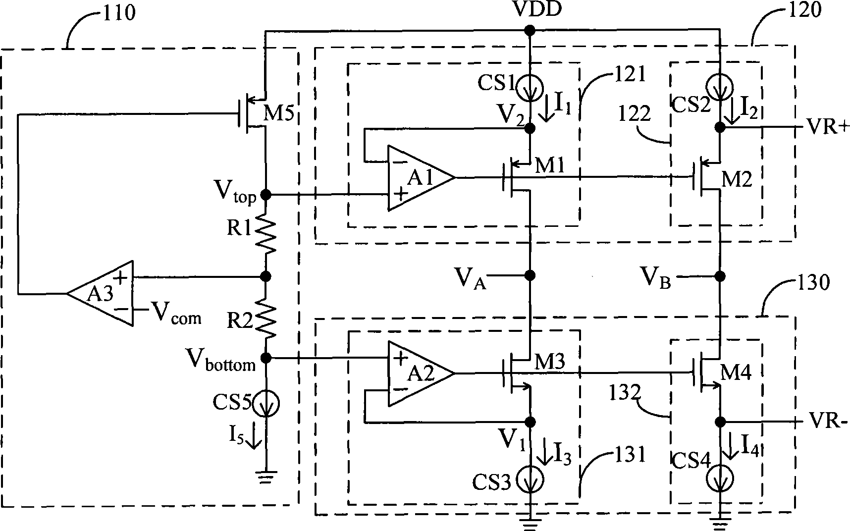
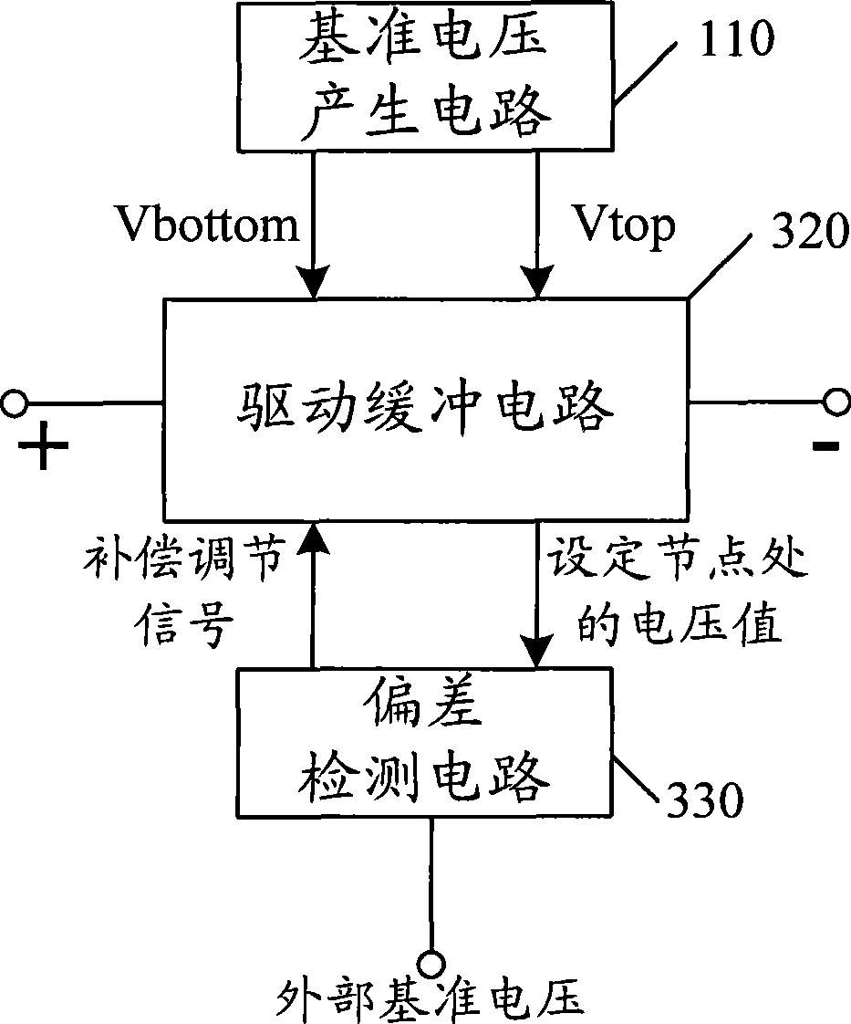
[0045] The composition structure of a reference voltage buffer circuit provided by the present invention is as follows: Figure 4 As shown, it includes: a reference voltage generation circuit 110, a drive buffer circuit 320 and a deviation detection circuit 330;

[0046] Wherein, the reference voltage generation circuit 110 is figure 1 The reference voltage generation circuit 110 in; the reference voltage generation circuit 110 generates the first initial voltage of the reference voltage at the common end (i.e. the D pole of the PMOS transistor) of the PMOS transistor and the resistor R1, and the first initial voltage of the resistor R2 and the current source CS3 The common terminal generates a reference voltage second initial voltage, and the reference voltages first initial voltage and second initial voltage are further provided to the driving buffer circuit 320 .

[0047] The driving buffer circuit 320 and figure 1 The combination of the first drive buffer circuit 120 and...

Embodiment 2

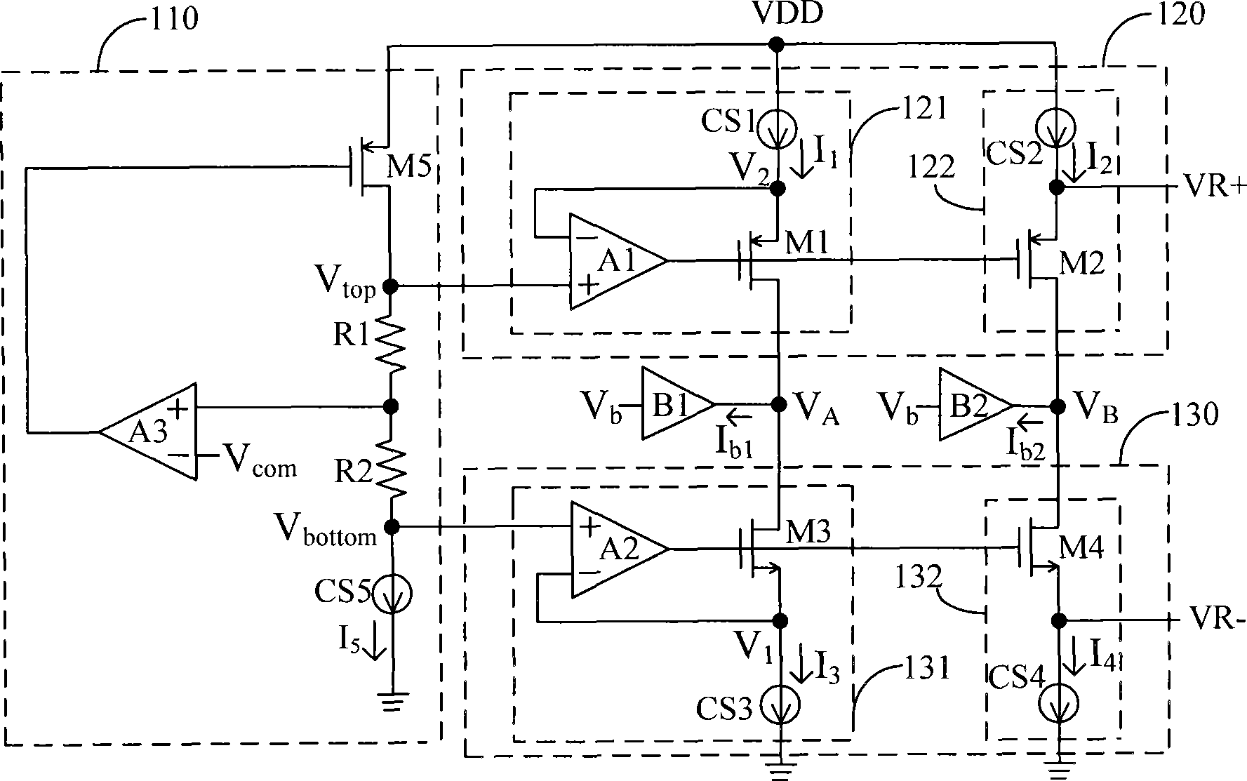
[0067] The present invention also provides another possible implementation of the reference voltage buffer circuit, the circuit structure of which is as follows Figure 5 As shown, it includes a reference voltage generation circuit 110, a drive buffer circuit 420 and a deviation detection circuit 330;

[0068] Among them, the reference voltage generation circuit 110 and the deviation detection circuit 330 are connected with Figure 4 The first embodiment shown is the same and will not be described in detail;

[0069] drive buffer circuit 420, whose circuit composition is compared to Figure 4 The implementation shown differs only in:

[0070] 1) at Figure 5 In this example, the Figure 4 Replace the voltage-controlled current source VCCS1 in the current source CS1 with the Figure 4 The voltage controlled current source VCCS2 in is replaced by the current source CS2;

[0071] 2) at Figure 5 In this example, the Figure 4The current source CS1 in is replaced by a volt...

Embodiment 3

[0083] The deviation detection circuit 330 in the above embodiment can also be realized by two circuits with identical structures and functions, such as Figure 6 As shown, it includes a reference voltage generation circuit 110, a drive buffer circuit 320, a first deviation detection circuit 531 and a second deviation detection circuit 532;

[0084] Among them, the reference voltage generating circuit 110 and the driving buffer circuit 320 are connected with Figure 4 The first embodiment shown is the same and will not be described in detail; the first deviation detection circuit 531 and the second deviation detection circuit 532 are each the same as the deviation detection circuit 330 in the first embodiment, and their circuit composition structure compared to Figure 4 The implementation shown differs only in:

[0085] exist Figure 6 In this example, the Figure 4 The nodes A and B in are disconnected and connected to the first deviation detection circuit 531 and the se...


PUM


Abstract

The present invention discloses a reference voltage buffer circuit, comprising a reference voltage generating circuit which generates and outputs a first primary voltage and a second primary voltage, and further comprising a driving buffer circuit and a deviation detecting circuit. The reference voltage buffer circuit provided by the embodiment of the present invention administers voltage adjustment to the given nodes of the driving buffer circuit through the deviation detecting circuit, realizing the adjustment and correction of the abnormal working state of a circuit, reliably solving the problem of reference voltage buffer circuit failing to work normally caused by production technique errors or other unpredictable factors, improving the production rate of standard quality of a circuit, providing reference voltage of great driving capacity, and achieving lower cost and circuit power dissipation.

Description

technical field [0001] The invention relates to reference voltage technology, in particular to a reference voltage buffer circuit. Background technique [0002] The reference voltage buffer circuit is a circuit that enhances the driving ability of the reference voltage, and it is widely used in various electronic devices. For example, in an Analog-Digital Converter (Analog-Digital Converter, ADC) / Digital-Analog Converter (Digital-Analog Converter, DAC), a high reference voltage (VR+) and a low reference voltage (VR-) are required as Reference standards, ADC / DAC utilizes these two reference standards to realize signal conversion. [0003] figure 1 It is a structural diagram of a conventional reference voltage buffer circuit, including: a reference voltage generating circuit 110 , a first driving buffer circuit 120 and a second driving buffer circuit 130 . [0004] The reference voltage generating circuit 110 further includes: an operational amplifier A3, a P-type Metal Oxi...

Claims


Application Information

Patent Timeline
Patent Type & Authority Applications(China)
IPC IPC(8): G05F1/46G05F1/56G05F1/563G01R19/165
Inventor 黄洪伟
Owner EZCHIPS MICROELECTRONICS CO LTD
Why Eureka
Try Eureka