Manufacturing method for realizing monolithic integration of microwave switch and logic control circuit thereof

A logic control circuit and monolithic integration technology, which is applied in the manufacture of circuits, electrical components, semiconductors/solid-state devices, etc., can solve the problems of wasting chip area, reducing the number of control ports of switching circuits, etc., and achieve simple wiring and reduce the number of control ports , the effect of saving chip area

Inactive Publication Date: 2010-09-15
天津中科海高微波技术有限公司
View PDF0 Cites 0 Cited by
  • Summary
  • Abstract
  • Description
  • Claims
  • Application Information

AI Technical Summary

Problems solved by technology

[0007] In view of this, the main purpose of the present invention is to provide a method for monolithic integration of microwave switches and their logic control circuits using GaAs E / DPHEMT technology, so as to solve the problem of excessive control signal leads in complex mobile phone systems. It leads to a large number of pads, which wastes most of the chip area. At the same time, a single power supply is used to greatly reduce the power consumption of the mobile phone. It is made into an SPDT MMIC with a built-in inverter logic circuit, which effectively reduces the number of control ports of the switch circuit.

Method used


Image

  • Manufacturing method for realizing monolithic integration of microwave switch and logic control circuit thereof
  • Manufacturing method for realizing monolithic integration of microwave switch and logic control circuit thereof
  • Manufacturing method for realizing monolithic integration of microwave switch and logic control circuit thereof

Examples


Embodiment Construction

[0039] In order to make the object, technical solution and advantages of the present invention clearer, the present invention will be described in further detail below in conjunction with specific embodiments and with reference to the accompanying drawings.

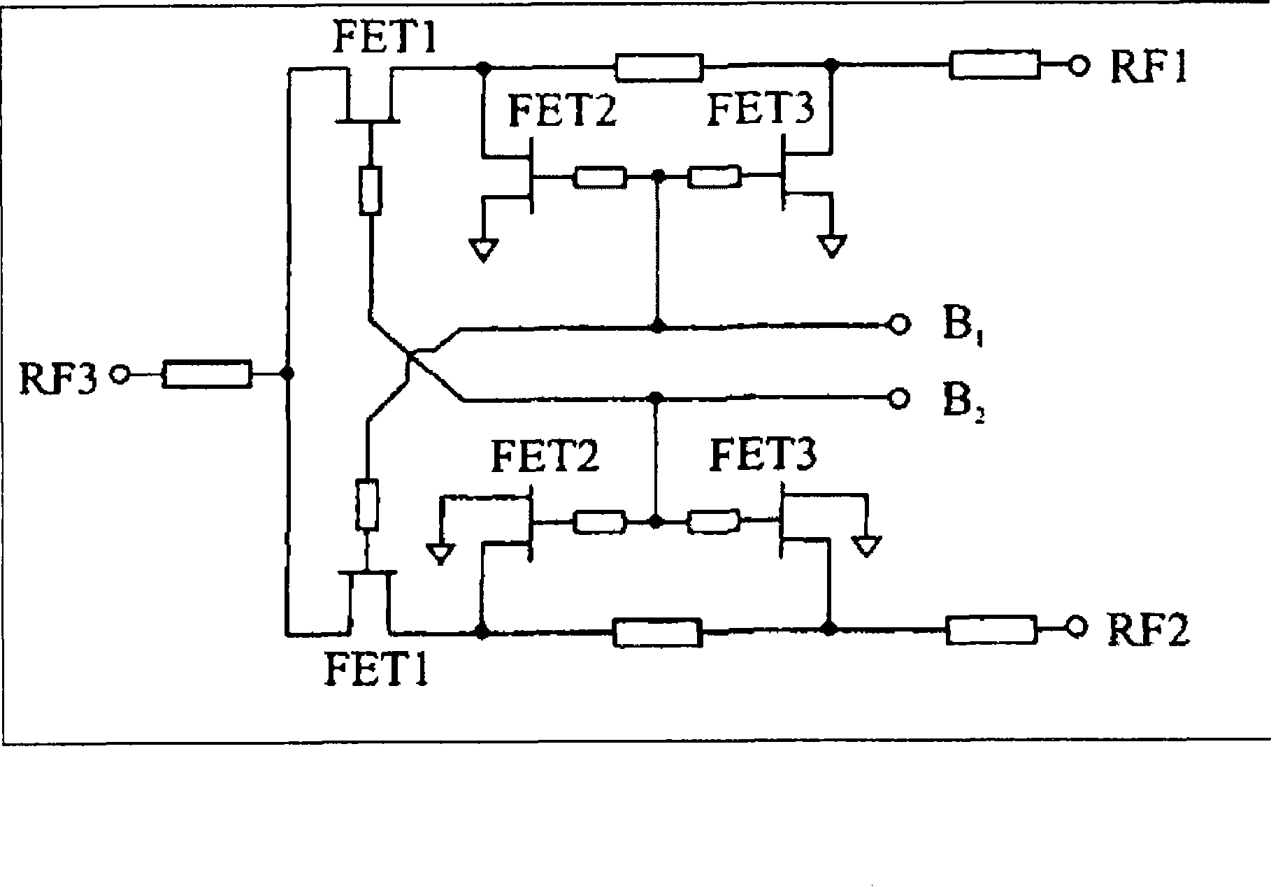
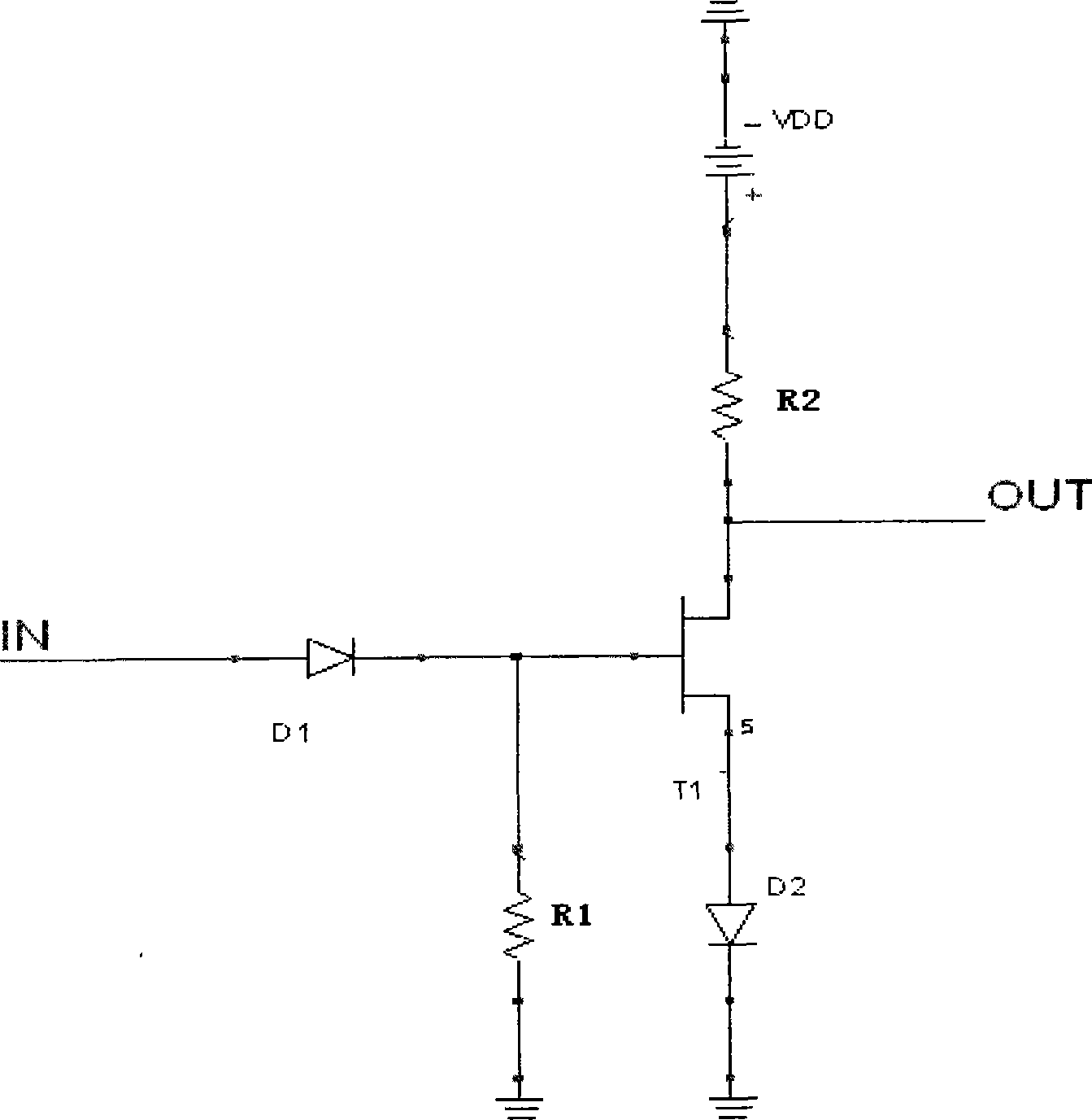
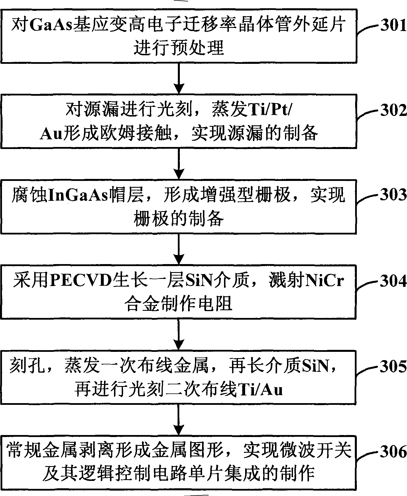
[0040] The manufacturing method of this invention using E / D PHEMT technology to realize the monolithic integration of microwave switch and its logic control circuit, considering the requirements of E / D PHEMT technology and integrated circuit testing, using E / D PHEMT materials and process, to make an inverter with a DCFL structure, and the control signal terminal of the SPDT switch is connected to the input and output terminals of the inverter on the chip, which is equivalent to the decoder built in the switch circuit, thereby reducing the single-pole double-throw The throw switch controls the number of ports, and the entire circuit only needs one control signal.

[0041] figure 1 Shows the schematic diagram of the single...


PUM


Abstract

The invention relates to the technical field of compound semiconductor MMIC, and discloses a manufacturing method for realizing monolithic integration of a microwave switch and a logic control circuit thereof by adopting a GaAs enhancement / depletion-type PHEMT technique. By utilizing a 1.0 mu m GaAs E / D PHEMT process, the method prepares a DC-10GHz SPDT MMIC with good performance, integrates a full-depletion-type microwave switch and an inverter logic circuit in the same chip, and basically realizes the integration of the logic circuit and a switching circuit. As the whole circuit only needs 1-bit control signals, the number of control ports of the switching circuit is effectively reduced, and the area of the chip is saved. The method lays a good foundation for adopting an E / D HEMT technique to realize the integration larger in scale and more complex in circuits in future. The method has the advantages of obvious effects, easy process design, economic applicability and high reliability, and is easy to adopt and popularize in the manufacture of microwave / millimeter-wave compound semiconductor circuits.

Description

technical field [0001] The invention relates to the technical field of compound semiconductor devices, in particular to a method for monolithically integrating a microwave switch and its logic control circuit by using GaAs-based E / D PHEMT technology. Background technique [0002] Microwave switches are key circuits in many microwave systems, and their applications range from sophisticated space communication systems to common electronic products such as mobile phones. As long as we switch the RF signal from one channel to another, or just need to change the on-off state of the RF signal, we need to use a microwave switch. Microwave switches with high performance, small size and versatility are widely used in various microwave systems. [0003] Microwave switches need to use logic circuits to control their on-off states during use. One method is to implement the two parts of the circuit with different chips, and connect the output port of the logic circuit with the control ...

Claims


Application Information

Patent Timeline
Patent Type & Authority Patents(China)
IPC IPC(8): H01L21/822
Inventor 黎明张海英徐静波付晓君
Owner 天津中科海高微波技术有限公司
Why Eureka
Try Eureka