Display panel substrate, display panel, display device and method for manufacturing display panel substrate

A technology for display panels and substrates, applied in identification devices, input/output processes of data processing, optics, etc., can solve problems such as rising manufacturing costs and reducing light transmittance, and achieve the effect of increasing aperture ratio and reducing manufacturing costs

Inactive Publication Date: 2009-10-14
SHARP KK
View PDF3 Cites 39 Cited by
  • Summary
  • Abstract
  • Description
  • Claims
  • Application Information

AI Technical Summary

Problems solved by technology

[0004] However, since the touch panel of Patent Document 1 must be attached to the front surface (screen) of the display device, there is a problem that the transmittance of light used for display decreases.
In addition, since a touch panel must be prepared separately in addition to the display device, there is a problem that the manufacturing cost increases accordingly.

Method used


Image

  • Display panel substrate, display panel, display device and method for manufacturing display panel substrate
  • Display panel substrate, display panel, display device and method for manufacturing display panel substrate
  • Display panel substrate, display panel, display device and method for manufacturing display panel substrate

Examples


Embodiment Construction

[0120] Below, refer to Figure 1 to Figure 25 , an embodiment of the present invention will be described.

[0121] (Example of structure of liquid crystal panel 1)

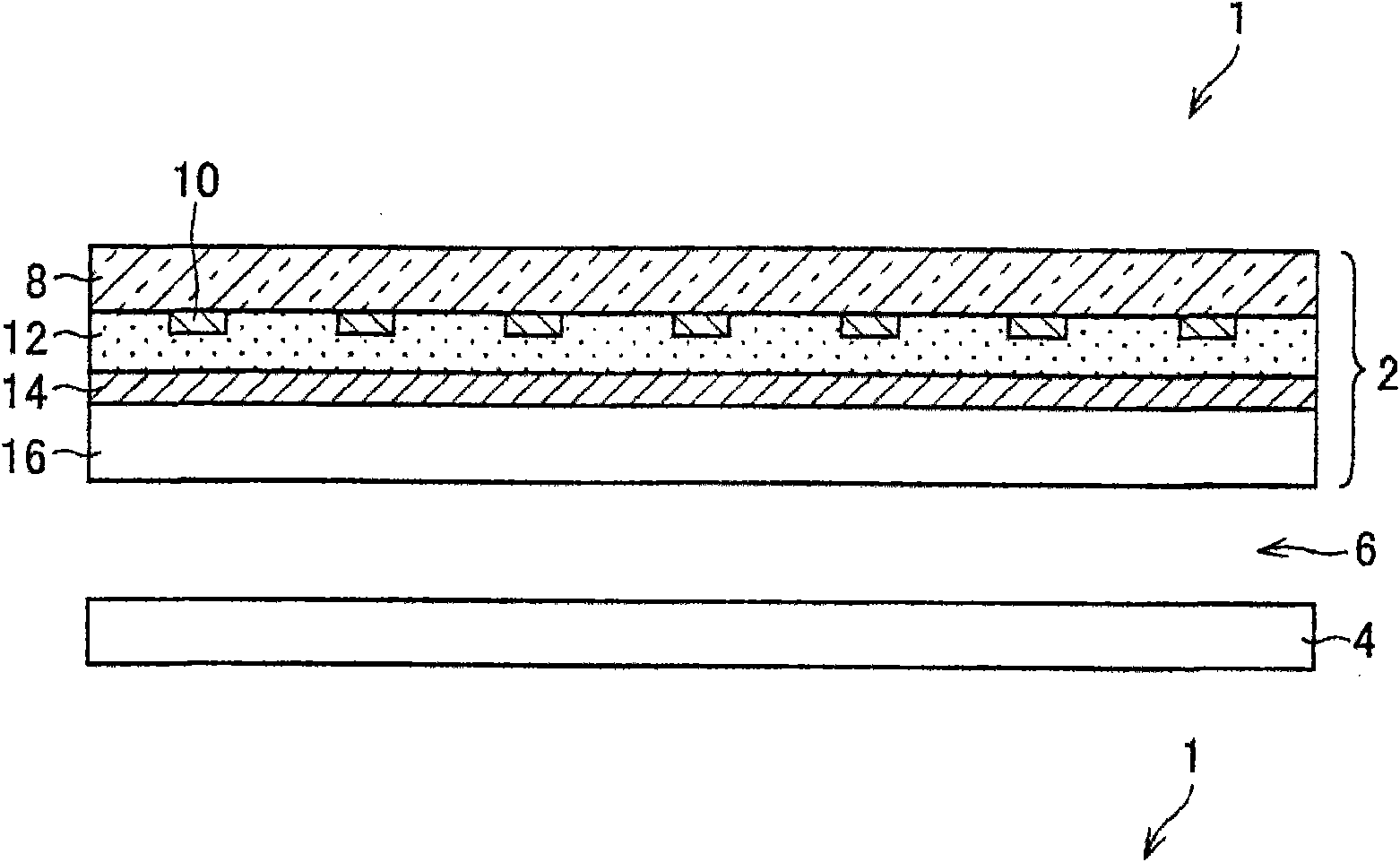
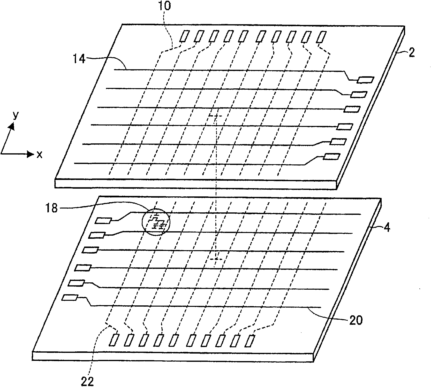
[0122] figure 1 It is a figure which shows the structure of the liquid crystal panel 1 (display panel) of this invention. As shown in the figure, the liquid crystal panel 1 is roughly composed of a counter substrate 2 (display panel substrate) having a touch panel function, and a TFT substrate 4 on which TFT elements are formed. Liquid crystal 6 (not shown) is injected between the counter substrate 2 and the TFT substrate 4 .

[0123] Such as figure 1 As shown, the opposite substrate 2 includes: a glass substrate 8 (insulating substrate), metal wiring 10 (first conductive wiring), piezoelectric film 12, metal wiring 14 (second conductive wiring), and a protective film16. The details will be described later, but with this structure, the counter substrate 2 functions as a touch panel.

[0124] (wiring on boar...


PUM


Abstract

A display panel substrate is provided with at least an insulating substrate; a first conductive wiring formed on the insulating substrate; a piezoelectric material film formed on the first conductive wiring; a second conductive wiring intersecting with the first conductive wiring; and protecting films for protecting the first conductive wiring, the second conductive wiring and the piezoelectric material film, respectively. The insulating film is formed at least in a region in an effective display region on the insulating substrate, and the piezoelectric film is formed at least on an intersecting point of the first conductive wiring and the second conductive wiring. Thus, the display panel substrate capable of integrating a touch panel function without increasing the sizes of the display panel is provided.

Description

technical field [0001] The present invention relates to a display panel substrate constituting a display panel, a display panel provided with the display panel substrate, a display device provided with the display panel, and a method of manufacturing the display panel substrate. Background technique [0002] In a display device, a so-called touch panel has conventionally been frequently used in order to allow easy operation while viewing a screen. The touch panel is usually pasted on the screen of the display device. The user performs various operations by pressing (selecting) objects such as buttons displayed on the screen through the touch panel. [0003] Patent Document 1 discloses a typical example of a touch panel attached to a display device. Patent Document 1 discloses a press detection unit (touch panel) having a structure in which a plurality of electrodes extending in the X direction are provided on one side of a piezoelectric body and, on the other side, a A pl...

Claims


Application Information

Patent Timeline
Patent Type & Authority Applications(China)
IPC IPC(8): G06F3/041G02F1/1333G09F9/00
CPCG02F1/13338G06F3/0414G06F3/047G06F3/04146
Inventor 村井淳人近间义雅高桥和树
Owner SHARP KK
Why Eureka
Try Eureka