Chip chuck

A chip and chuck technology, applied in the field of chip chucks, can solve problems such as low efficiency, chip breakdown, affecting chip yield, etc., and achieve the effect of avoiding electrostatic breakdown and meeting the requirements of efficiency

Inactive Publication Date: 2009-10-28
SEMICON MFG INT (SHANGHAI) CORP
View PDF0 Cites 3 Cited by
  • Summary
  • Abstract
  • Description
  • Claims
  • Application Information

AI Technical Summary

Problems solved by technology

[0004] In this step, the pins of the chip placed on the chip chuck are suspended, so the chip is easily broken down by the static electricity carried by the equipment or the operator, thus affecting the yield of the c

Method used


Image

  • Chip chuck
  • Chip chuck
  • Chip chuck

Examples


Embodiment Construction

[0016] The specific implementation of the chip chuck provided by the present invention will be described in detail below in conjunction with the accompanying drawings.

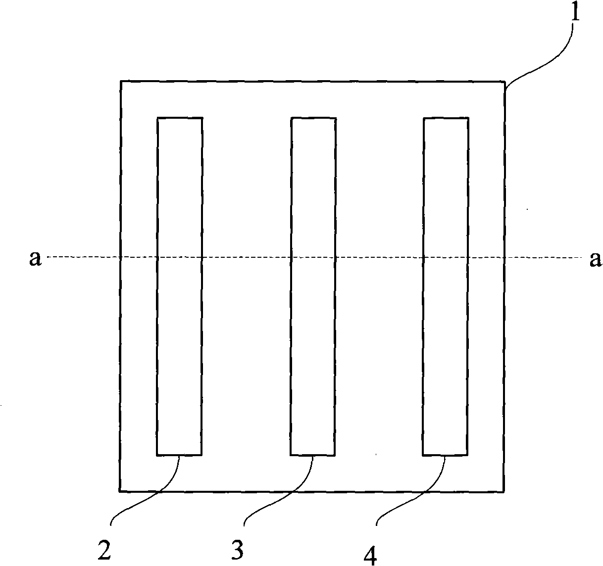
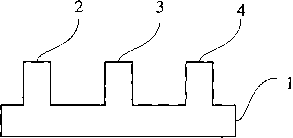
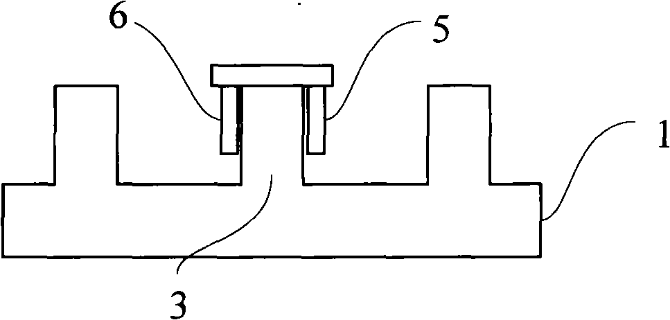
[0017] attached Figure 4 Shown is a schematic cross-sectional view of the chuck structure of the first specific embodiment of the chip chuck according to the present invention. It includes a base 101, a chip holder 102 on the surface of the base 101, and a target chip placed thereon. According to actual needs, more brackets can also be designed on the surface of the base 101 . The top portion 120 of the chip carrier 102 is attached Figure 4 For the portion above the middle dotted line, the interface of the top portion 120 has a narrow top and a wide bottom.

[0018] When the target chip is not placed on the chip chuck, the two rows of pins 111 and 112 of the chip are parallel to each other, and the distance between the roots of the two rows of pins 111 and 112 is the distance between the two rows of pins....


PUM


Abstract

The invention relates to a chip chuck which comprises a base and a chip bracket positioned on the surface of the base, wherein the section of the top end part of the chip bracket forms a shape with a narrow upper part and a wide lower part; when a target chip is not arranged on the chip chuck, the width of the upper edge of the top end part is less than the distance between two rows of pins of the target chip, and the width of the lower edge is larger than the distance between two rows of pins of the target chip; the height of the top end part is less than the length of the pins of the target chip; and the base and the chip bracket are made of conductive materials and are both grounded. The invention has the advantages that the provided chip chuck can conveniently earth the pins of the chip fast, avoids electrostatic breakdown and meets the requirement of large-scale production to efficiency.

Description

【Technical field】 [0001] The invention relates to semiconductor packaging technology, in particular to a chip chuck capable of preventing electrostatic breakdown. 【Background technique】 [0002] Wire bonding is an indispensable link in semiconductor packaging technology. The usual wire bonding technology is to place the chip on a wire chuck and use special wire bonding equipment for wire bonding. [0003] attached figure 1 Shown is a top view of a conventional chip chuck, including a base 1 and chip holders 2 , 3 and 4 located on the surface of the base 1 . According to actual needs, more chip trays can also be designed. attached figure 2 shown attached figure 1 The cross-sectional view of the chip chuck along the a-a direction. The sidewalls of chip trays 2, 3 and 4 are vertical, and the width of the chip tray is smaller than the distance between two rows of pins of the target chip, so as to ensure that the chip can be placed on the chip tray smoothly. attached im...

Claims


Application Information

Patent Timeline
IPC IPC(8): H01L21/683H01L21/60H05F3/02
Inventor 王炯
Owner SEMICON MFG INT (SHANGHAI) CORP
Why Eureka
Try Eureka