High-brightness light emitting diode with GaN-based multiquantum-well structure and preparation method thereof

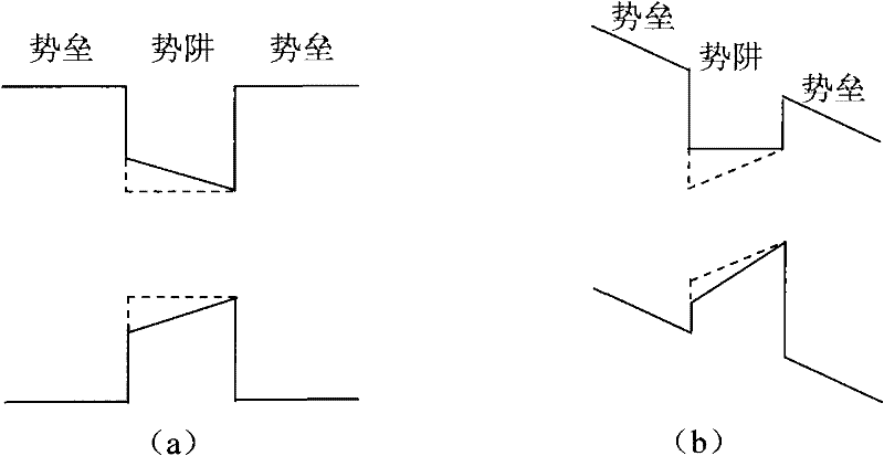
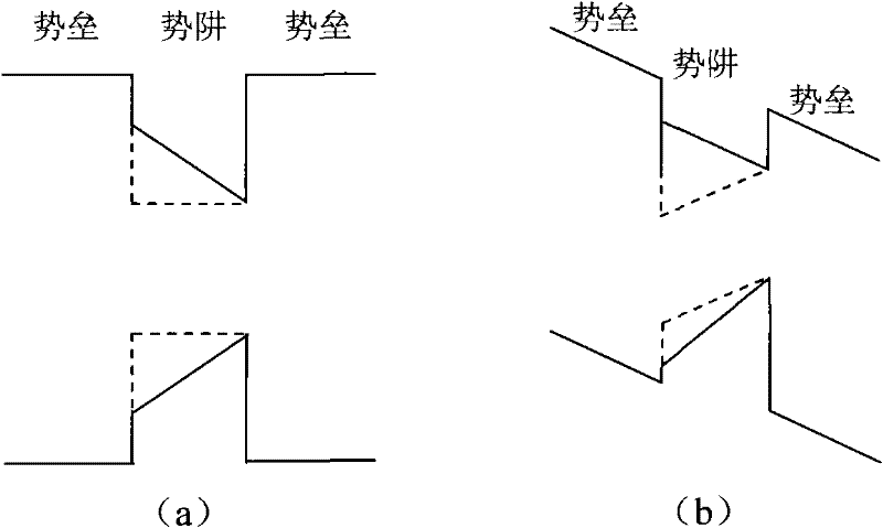
A technology of light-emitting diodes and multiple quantum wells, which is applied in the direction of electrical components, circuits, semiconductor devices, etc., can solve the problems of small electron and hole radiation recombination probability and low luminous intensity, so as to suppress wavelength drift, enhance confinement, and improve The effect of luminous efficiency

Inactive Publication Date: 2011-06-08
EPITOP PHOTOELECTRIC TECH
View PDF0 Cites 0 Cited by
  • Summary
  • Abstract
  • Description
  • Claims
  • Application Information

AI Technical Summary

Problems solved by technology

[0007] The object of the present invention is to provide a GaN-based multi-quantum well structure high-brightness light-emitting diode and its Preparation

Method used


Image

  • High-brightness light emitting diode with GaN-based multiquantum-well structure and preparation method thereof
  • High-brightness light emitting diode with GaN-based multiquantum-well structure and preparation method thereof
  • High-brightness light emitting diode with GaN-based multiquantum-well structure and preparation method thereof

Examples


Embodiment 1

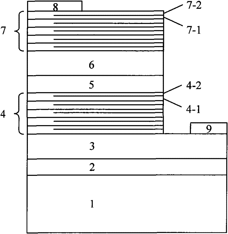
[0040] 1. Put the no-clean (0001) surface sapphire substrate into the reaction chamber, 2 Under atmosphere, heat to 1050°C and bake for 10 minutes, and the pressure in the reaction chamber is 50 Torr.

[0041] 2. Grow a GaN buffer layer with a thickness of 10nm at 500°C, the growth pressure is 500Torr, the flow rate of carrier gas is 10L / min, the flow rate of TMGa is 20μmol / min, NH 3 The flow rate is 80mol / min.

[0042] 3. Grow an n-type silicon-doped GaN layer with a thickness of 2 μm at 950 ° C, the growth pressure is 100 Torr, the flow rate of carrier gas is 5 L / min, the flow rate of TMGa is 50 μmol / min, NH 3 The flow rate is 120mol / min, SiH 4 The flow rate is 0.2nmol / min.

[0043] 4. Then in N 2 Three periods of InGaN / GaN quantum wells were grown under the atmosphere, and the growth pressure was 50Torr. The well layer is InGaN, the thickness is 2nm, the flow rate of TMGa is 1μmol / min, the flow rate of TMIn is 10μmol / min, NH 3 The flow rate is 120mol / min, the growth t...

Embodiment 2

[0050] 1. Put the no-clean (0001) surface sapphire substrate into the reaction chamber, and 2 Heat to 1080° C. and bake for 12 minutes under atmosphere, and the pressure in the reaction chamber is 50 Torr.

[0051] 2. Grow a GaN buffer layer with a thickness of 15nm at 530°C, the growth pressure is 520Torr, the flow rate of carrier gas is 15L / min, the flow rate of TMGa is 30μmol / min, NH 3 The flow rate is 100mol / min.

[0052] 3. Grow an n-type silicon-doped GaN layer with a thickness of 2.3 μm at 980 ° C, the growth pressure is 150 Torr, the flow rate of carrier gas is 8 L / min, the flow rate of TMGa is 100 μmol / min, NH 3 The flow rate is 250mol / min, SiH 4 The flow rate is 0.5 nmol / min.

[0053] 4. Then in N 2 Four periods of InGaN / GaN quantum wells were grown under the atmosphere, and the growth pressure was 100Torr. The well layer is InGaN, the thickness is 3nm, the flow rate of TMGa is 2μmol / min, the flow rate of TMIn is 15μmol / min, NH 3 The flow rate is 250mol / min, th...

Embodiment 3

[0058] 1. Put the no-clean (0001) surface sapphire substrate into the reaction chamber, and 2 Under atmosphere, heat to 1100°C and bake for 15 minutes, and the reaction chamber pressure is 50 Torr.

[0059] 2. Grow a GaN buffer layer with a thickness of 20nm at 550°C, the growth pressure is 530Torr, the flow rate of carrier gas is 18L / min, the flow rate of TMGa is 40μmol / min, NH 3 The flow rate is 120mol / min.

[0060] 3. Grow an n-type silicon-doped GaN layer with a thickness of 2.5 μm at 1000 ° C, the growth pressure is 200 Torr, the flow rate of carrier gas is 10 L / min, the flow rate of TMGa is 120 μmol / min, NH 3 The flow rate is 280mol / min, SiH 4 The flow rate is 1 nmol / min.

[0061] 4. Then in N 2 InGaN / GaN quantum wells were grown for 5 periods under the atmosphere, and the growth pressure was 200Torr. The well layer is InGaN, the thickness is 4nm, the flow rate of TMGa is 3μmol / min, the flow rate of TMIn is 20μmol / min, NH 3 The flow rate is 350mol / min, the growth t...


PUM


Abstract

The invention discloses a high-brightness light emitting diode with a GaN-based multiquantum-well structure and a preparation method thereof, and relates to a light emitting diode. The light emitting diode comprises a substrate, a low temperature buffer layer, an n-type doped GaN layer, 3 to 5 InGaN / GaN multiquantum wells, a p-type doped AlGaN layer, a p-type doped CaN layer, 5 periodic p-InGaN / p-AlGaN superlattice layers, a p-type ohmic contact layer and an n-type ohmic contact layer prepared on the n-type doped GaN layer in turn from bottom to top. The preparation method comprises the following steps: putting the substrate into a reaction chamber to perform thermal treatment for growing a GaN buffer layer, an n-type silicon-doped GaN layer, 3 to 5 periodic InGaN / GaN multiquantum wells with graded components, a p-type Mg-doped AlGaN layer, a p-type Mg-doped GaN layer and 5 periodic Mg-doped p-InGaN / p-AlGaN superlattice layers in turn; performing annealing after epitaxial growth; etching an n-type GaN layer; and preparing the n-type and the p-type ohmic contact layers.

Description

technical field [0001] The invention relates to a light-emitting diode, in particular to a high-brightness light-emitting diode (LED) with a GaN-based multi-quantum well structure. Background technique [0002] Wide bandgap Group III nitrides are a semiconductor material system that has been studied more actively recently. Semiconductor microstructure materials composed of group III nitrides and their continuously changing solid solution alloys have large band gap, high electron drift saturation velocity, strong breakdown field, small dielectric constant, good thermal conductivity, and high temperature resistance , anti-corrosion and other advantages ([1]S Nakamura, M Senoh, N Iwasaand S Nagahama, 1995Appl.Phys.Lett.67, 1868), it has extremely bright application prospects in the production of short-wavelength light-emitting devices. In particular, semiconductor lighting sources represented by high-brightness GaN-based LEDs have the advantages of small size, environmental pr...

Claims


Application Information

Patent Timeline
Patent Type & Authority Patents(China)
IPC IPC(8): H01L33/00
Inventor 刘宝林李晓莹
Owner EPITOP PHOTOELECTRIC TECH
Why Eureka
Try Eureka