Epitaxial wafer for gallium-nitride-based light emitting diode, and preparation method for epitaxial wafer

A light-emitting diode, gallium nitride-based technology, applied in the direction of electrical components, circuits, semiconductor devices, etc., can solve the problems of reducing the luminous efficiency of light-emitting diodes, and achieve the effect of improving the ability of compound light emission, shortening the transmission distance, and improving the luminous efficiency

Active Publication Date: 2017-06-20
HC SEMITEK ZHEJIANG CO LTD
View PDF4 Cites 5 Cited by
  • Summary
  • Abstract
  • Description
  • Claims
  • Application Information

AI Technical Summary

Problems solved by technology

[0006] In order to solve the problem of reducing the luminous efficiency of light-emitting diodes in the prior art, an embodiment of the present invention provides an epitaxial wafer of a gallium nitride-based light-emitting diode and a preparation method thereof

Method used


Image

  • Epitaxial wafer for gallium-nitride-based light emitting diode, and preparation method for epitaxial wafer
  • Epitaxial wafer for gallium-nitride-based light emitting diode, and preparation method for epitaxial wafer
  • Epitaxial wafer for gallium-nitride-based light emitting diode, and preparation method for epitaxial wafer

Examples


Embodiment 1

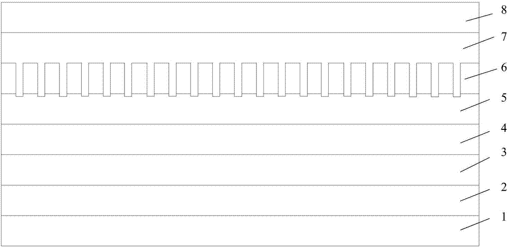
[0035] An embodiment of the present invention provides an epitaxial wafer of a gallium nitride-based light-emitting diode, see figure 1 , the epitaxial wafer includes a sapphire substrate 1, and a GaN buffer layer 2, an undoped GaN layer 3, an N-type GaN layer 4, a multi-quantum well layer 5, a P-type AlGaN layer 6, P-type GaN layer 7 .

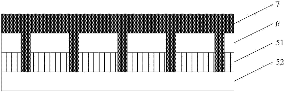
[0036] In this embodiment, the multi-quantum well layer is formed by sequentially stacking a plurality of sub-layers, and each sub-layer includes a quantum well layer and a quantum barrier layer stacked on the quantum well layer. like figure 2 As shown, there are several through holes in the P-type AlGaN layer 6 and the quantum barrier layer 51 closest to the P-type AlGaN layer. The quantum well layer 52 of the AlGaN layer, and the P-type GaN layer 7 are filled in the through hole.

[0037] Optionally, the cross-section of the through hole perpendicular to the stacking direction of the epitaxial wafers may be square, circular, star-shaped...

Embodiment 2

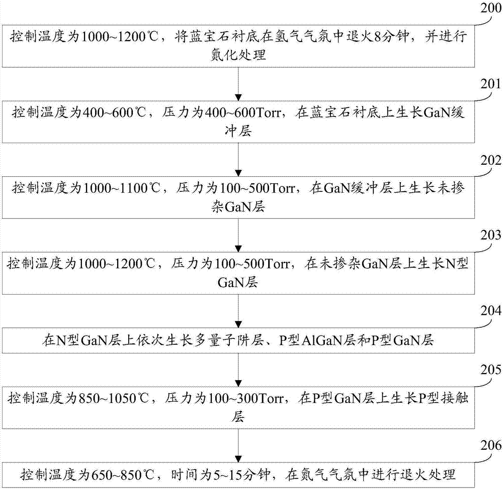
[0053] An embodiment of the present invention provides a method for preparing an epitaxial wafer of a gallium nitride-based light-emitting diode, which is suitable for preparing the epitaxial wafer provided in Embodiment 1. See image 3 , the preparation method comprises:

[0054] Step 200: Control the temperature to 1000-1200° C., anneal the sapphire substrate in a hydrogen atmosphere for 8 minutes, and perform nitriding treatment.

[0055] Understandably, step 200 can clean the surface of the sapphire substrate.

[0056] In this embodiment, the sapphire substrate 1 adopts (0001) crystal orientation sapphire.

[0057] Step 201: Control the temperature to 400-600° C. and the pressure to 400-600 Torr to grow a GaN buffer layer on the sapphire substrate.

[0058] Optionally, the thickness of the GaN buffer layer may be 15-35 nm.

[0059] Optionally, after step 201, the preparation method may further include:

[0060] The control temperature is 1000-1200° C., the pressure is ...


PUM


Abstract

The invention discloses an epitaxial wafer for a gallium-nitride-based light emitting diode, and a preparation method for an epitaxial wafer, and belongs to the technical field of semiconductors. The epitaxial wafer comprises a sapphire substrate, a GaN buffering layer, a non-doped GaN layer, an N-type GaN layer, a multi-quantum-well layer, a P-type AlGaN layer and a P-type GaN layer. The multi-quantum-well layer is formed by the sequential stacking of a plurality of sublayers, and each sublayer comprises a quantum well layer and a quantum barrier layer staked on the quantum well layer. The interior of the P-type AlGaN layer and the interior of the quantum barrier layer nearest to the P-type AlGaN layer are provided with a plurality of through holes. The through holes extend to the quantum well layer nearest to the P-type AlGaN layer in a direction opposite to the stacking direction of the epitaxial wafer. The P-type AlGaN layer is disposed in the through holes. The epitaxial wafer improves the longitudinal hole transmission, improves the composite illuminating capability of a hole injection quantum well, and improves the hole mobility.

Description

technical field [0001] The invention relates to the technical field of semiconductors, in particular to an epitaxial wafer of a gallium nitride-based light-emitting diode and a preparation method thereof. Background technique [0002] Light Emitting Diode (English: Light Emitting Diode, LED for short) is a semiconductor device capable of effectively converting electrical energy into light energy. At present, gallium nitride-based LEDs have received more and more attention and research. [0003] The epitaxial wafer of a GaN-based LED includes a sapphire substrate, a GaN buffer layer, an undoped GaN layer, an N-type GaN layer, and a multiple quantum well layer (English: Multiple Quantum Well, referred to as: MQW) stacked on the sapphire substrate in sequence. , P-type AlGaN layer, and P-type GaN layer. When a current flows, the electrons in the N-type GaN layer and the holes in the P-type GaN layer enter the multi-quantum well layer to recombine and emit light. [0004] In t...

Claims


Application Information

Patent Timeline
Patent Type & Authority Applications(China)
IPC IPC(8): H01L33/06H01L33/20H01L33/12H01L33/32H01L33/00
CPCH01L33/0075H01L33/06H01L33/12H01L33/20H01L33/32
Inventor 王群董彬忠李鹏王江波
Owner HC SEMITEK ZHEJIANG CO LTD
Why Eureka
Try Eureka