LED light source unit

A technology of LED light source and adhesive tape, applied in optics, electrical components, nonlinear optics, etc., can solve the problems of inability to use, not considered, increase the substrate, etc., and achieve the effect of suppressing the reduction of luminous efficiency and preventing the loss of LEDs

Inactive Publication Date: 2009-12-02
DENKA CO LTD
View PDF5 Cites 14 Cited by
  • Summary
  • Abstract
  • Description
  • Claims
  • Application Information

AI Technical Summary

Problems solved by technology

However, it is necessary to increase the thickness of the substrate. In addition, compared with the printed circuit board, it is necessary to increase the size punched from the electrodes and wiring patterns, etc., so there is a problem that the substrate area becomes larger.
In addition, since the part other than the LED mounting part cannot be bent arbitrarily, the formation position of the input terminal, etc. is restricted.
[0012] In addition, if the thickness of the metal base plate of the above-mentioned metal base circuit board is reduced to form a small-sized structure punched from electrodes and wiring patterns, etc. similarly to the printed board, then the same as the printed board formed with through holes, due to No consideration is given to heat dissipation from the back of the metal base plate to the housing. In the case of continuous lighting of the LED, there is a problem that the luminous efficiency of the LED itself decreases as the temperature of the LED increases.
In addition, if the metal base circuit board is slightly bent, the insulating layer will crack and cannot be used. In addition, there are problems such as that the LED mounting part cannot be bent arbitrarily.

Method used


Image

  • LED light source unit
  • LED light source unit
  • LED light source unit

Examples


Embodiment 1

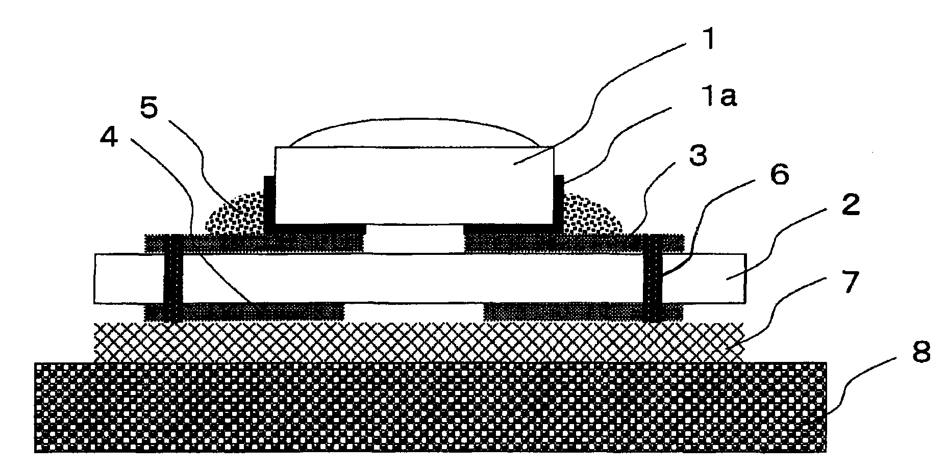
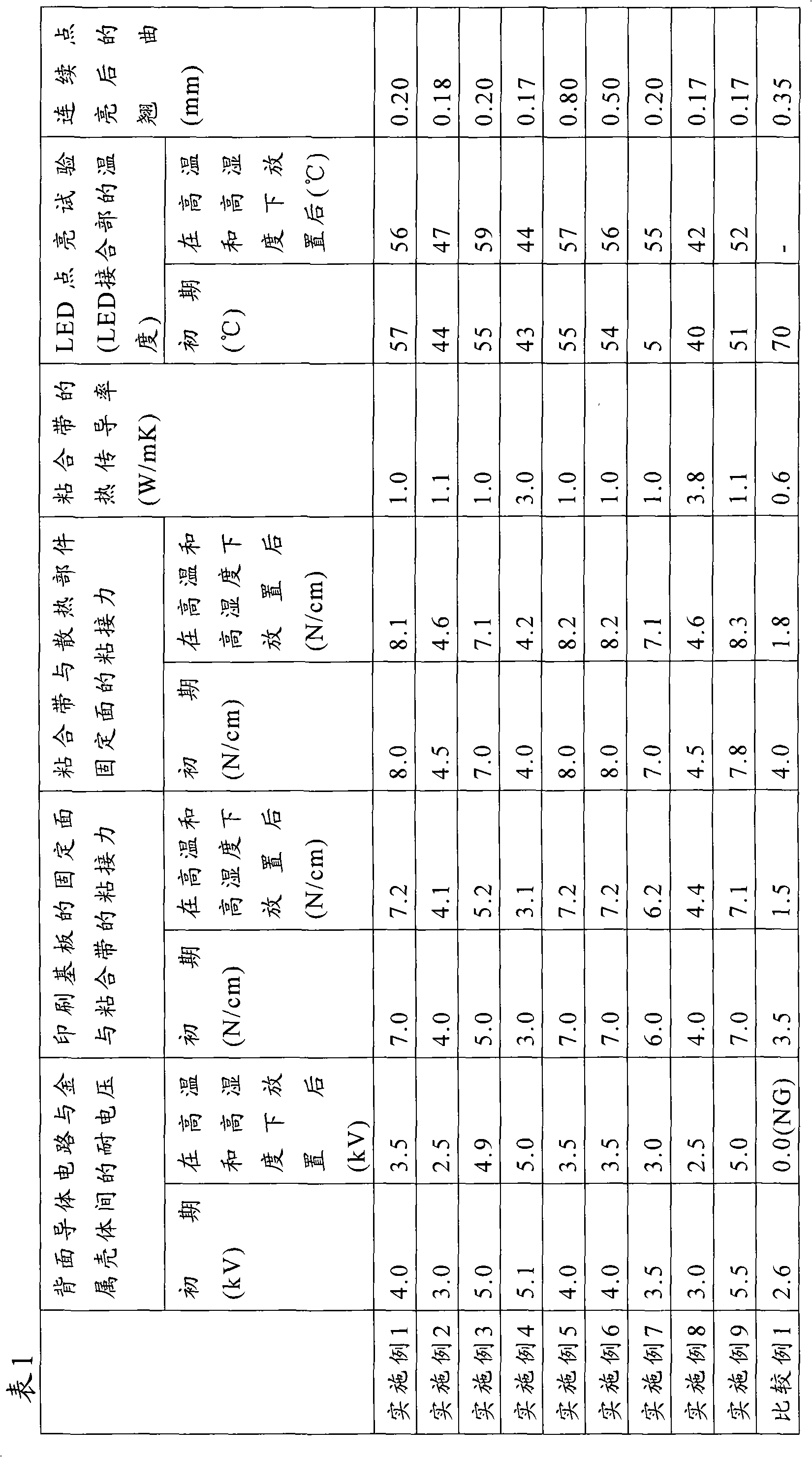
[0101] make figure 1 LED light source unit of the type shown. That is, a 35 μm thick copper foil is formed on both sides of an epoxy resin cloth impregnated with a glass substrate with a thickness of 100 μm, and a predetermined position of a printed circuit board with glass cloth (the conductor circuit connected to the LED electrode terminal 1a and the conductor circuit located at the conductor The position where the conductor circuit on the back of the circuit is connected) forms a through hole, and after copper plating, a conductor circuit for mounting LEDs, a conductor circuit for LED lighting and heat dissipation on the back are formed, and a printed circuit board is made.

[0102] 10% by mass of acrylic acid was mixed in 90% by mass of 2-ethylhexyl acrylate ("2EHA" manufactured by Toagosei Co., Ltd.) dissolved with 10% by mass of acrylic rubber ("AR-53L" manufactured by Nippon Zesai Co., Ltd.) ("AA" manufactured by Toagosei Co., Ltd.), and 0.5% by mass of photopolymeriz...

Embodiment 2

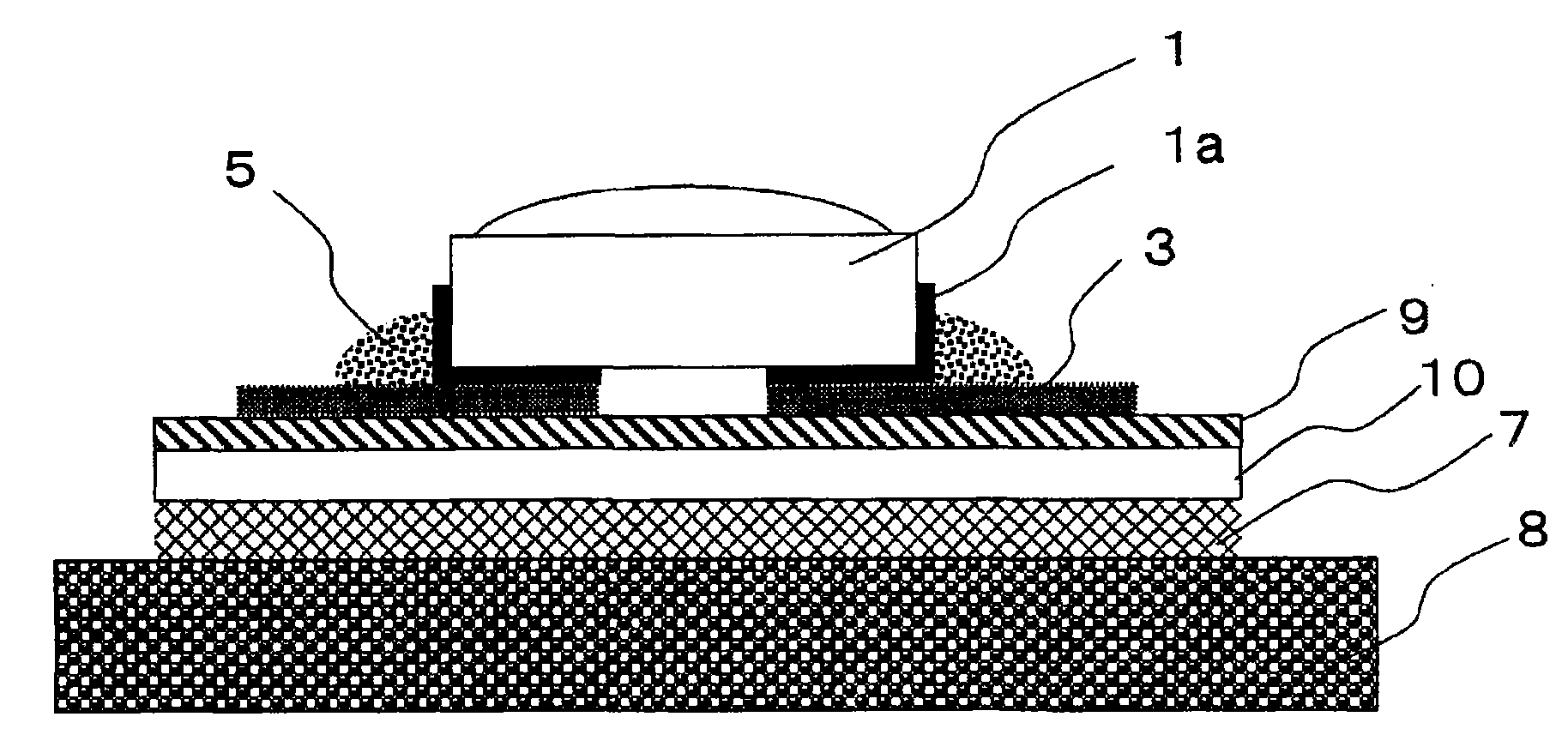
[0129] An LED light source unit was fabricated in the same manner as in Example 1 except for the following points. That is, as the inorganic filler, an inorganic filler A having a maximum particle diameter of 45 μm or less and an average particle diameter of 9 μm obtained by classifying alumina (“DAW-10” manufactured by Denki Kagaku Kogyo Co., Ltd.) through a 45 μm sieve was used. Then, the resin composition D was obtained by mixing the inorganic filler A at a compounding ratio of 40% by volume, the resin composition A at 45% by volume, and the resin composition B at 15% by volume.

[0130] Next, the defoaming-treated resin composition D was coated on a 75 μm-thick PET film whose surface was subjected to a release treatment, and the PET film on which the surface was subjected to a release treatment was further coated, and 3000 mJ was irradiated from the front and back sides. / cm 2 Ultraviolet rays with a wavelength of 365nm. Thereafter, heat treatment was performed at 100° C...

Embodiment 3

[0134] An LED light source unit was fabricated in the same manner as in Example 1 except for the following points. That is, using the same resin composition D as used in Example 2, the defoaming-treated resin composition was applied to a thickness of 46 μm on a 75-μm-thick PET film whose surface was subjected to a release treatment. D, a glass cloth with a thickness of 50 μm was laminated thereon, a PET film whose surface was subjected to a mold release treatment was further coated on the glass cloth, and the resin composition D was impregnated in the glass cloth by lamination.

[0135] Next, irradiate 3000mJ / cm from the front and back 2 Ultraviolet rays with a wavelength of 365nm. Then, heat processing was performed at 100 degreeC for 3 hours, resin composition D was hardened, and the electrically insulating heat conductive adhesive tape of thickness 150 micrometers was obtained.

[0136] Next, apply cream solder ("M705" manufactured by Senju Metal Co., Ltd.) to the predete...


PUM

PropertyMeasurementUnit
thicknessaaaaaaaaaa
thicknessaaaaaaaaaa
particle sizeaaaaaaaaaa

Abstract

An LED light source unit having excellent heat dissipation properties, preventing damage on an LED, illuminating brightly, and having a long service life. The LED light source unit has a printed circuit board, one or more light emitting diodes mounted on the printed circuit board, and an adhesive tape for fixing the printed circuit board to the surface of a heat dissipation member. The LED light source unit is characterized in that the heat conductivity of the tape is 1 to 4 W / mK, and the withstand voltage between a rear surface conductor circuit and a metal casing is 1.0 kV or higher.

Description

technical field [0001] The present invention relates to a light emitting diode (LED) light source unit using a light emitting diode (LED) as a light source, excellent in heat dissipation, and long in life. Background technique [0002] In a liquid crystal display device or the like composed of a liquid crystal display element and a backlight, a small fluorescent tube called a CCFL (cold cathode tube) is generally used as a light source of the backlight. [0003] The light source of the aforementioned CCFL (cold cathode tube) adopts the following structure: mercury is sealed in the discharge tube, and the mercury is excited by discharge to release ultraviolet rays. Therefore, recently, an alternative light source that does not use harmful mercury has been demanded from the viewpoint of the environment. [0004] Recently, LED light source units using light emitting diodes (LEDs) as light sources have come into use in many fields. [0005] For example, as a new light source f...

Claims


Application Information

Patent Timeline
Patent Type & Authority Applications(China)
IPC IPC(8): H01L33/00C09J7/02C09J11/04C09J133/02H01L33/62H01L33/64
CPCH05K3/386G02F2001/133628H05K2201/10106C09J133/02C09J2205/102C09J2483/006H05K2201/0209H05K1/056G02F1/133603C08K3/22C08K7/00H05K1/0206H05K2203/0191H05K3/0061C09J7/0282C09J2433/00C09J7/25C09J2301/408G02F1/133628
Inventor 八岛克宪宫川健志宫田建治西太树冈岛芳彦冈田拓也高野敬司光永敏胜
Owner DENKA CO LTD
Why Eureka
Try Eureka