

Monopole inverter capable of boosting voltage
An inverter, single-stage technology, applied in the field of new single-stage boostable inverters, can solve the problems of not making full use of capacitor voltage levels, easily causing resonance, increasing system costs, etc., and achieving large-voltage differential power transfer. Transfer, avoid output current waveform distortion, reduce the effect of the number of switches
- Summary
- Abstract
- Description
- Claims
- Application Information
AI Technical Summary
Problems solved by technology
Method used
Image

Examples
Embodiment Construction
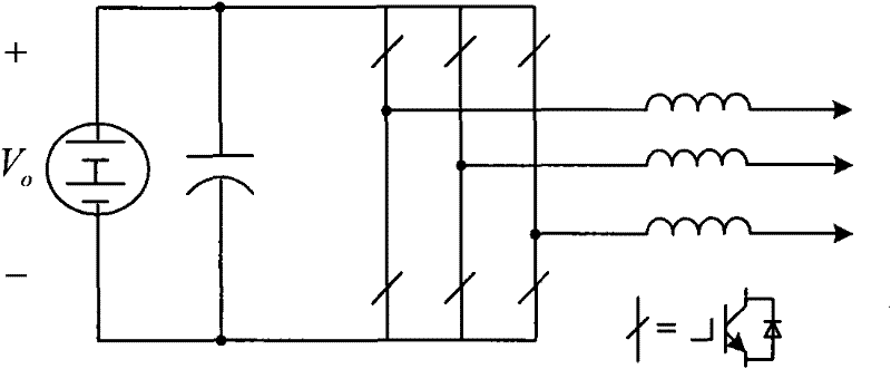
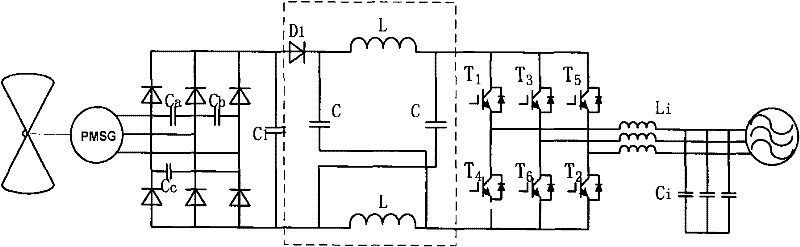
[0031] as attached Figure 4 As shown, in addition to the three-phase switching bridge (B) of the traditional voltage-type inverter, the novel single-stage boostable inverter topology of the present invention adds a boost inductor (the The terminal with the same name is marked in the figure), capacitor (C), blocking diode (D), and switch tube (T) for energy feedback channel (can be omitted if no energy feedback is required). One end of the primary winding (L1) is positively connected to the DC power supply, and the other end is connected in series with a reverse blocking diode (D), connected to one end of the secondary winding (L2) and positively connected to the DC bus of the inverter bridge (B). The other end of the secondary winding (L2) is connected in series with the positive pole of the capacitor (C), the negative pole of the capacitor (C) is connected to the negative terminal of the DC bus of the inverter bridge (B), and then connected to the negative pole of the power ...
PUM
 Abstract
Description
Claims
Application Information