


Quick Research
Generate reliable direction feasibility study reports for your R&D in just a few steps.

Technical Q&A
Discover and master advanced knowledge NOW. Basics, ideas, possibilities, all at once.

Find Solutions
As an expert in R&D theories, this can generate solutions to your technical problems instantly.

Evaluate Feasibility
Analyze your overall solution with one click, know your potential R&D risks in advance.

Monitor Landscape
Get weekly tech updates, stay abreast of the latest tech innovations and key insights.
Wafer processing method
A chip processing, chip technology, applied in the direction of stone processing equipment, laser welding equipment, electrical components, etc., can solve uneconomical problems
- Summary
- Abstract
- Description
- Claims
- Application Information
AI Technical Summary
Problems solved by technology
Method used
Image

Examples
Embodiment Construction
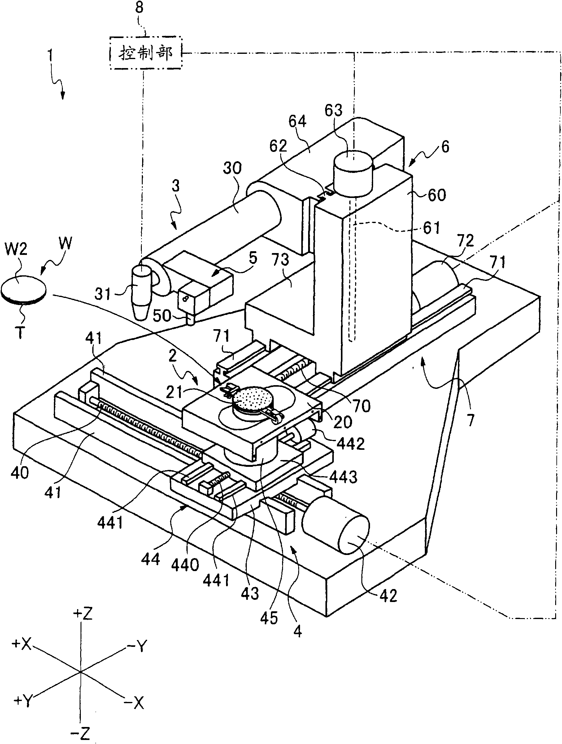
[0021] figure 1 The shown laser processing apparatus 1 is an apparatus capable of processing a wafer by irradiating laser light to form a degenerated layer inside it, and the laser processing apparatus 1 includes: a chuck table 2 that holds a wafer as an object to be processed and a laser irradiation member 3 for irradiating the workpiece held on the chuck table 2 with laser light for processing.
[0022] The chuck table 2 is subjected to machining feeding in the X-axis direction by the machining feeding member 4 . The processing feed member 4 is a member for processing the chuck table 2 and the laser irradiation member 3 in the direction of the X-axis, and the processing feed member 4 includes a ball screw 40 arranged on the X-axis. direction; a pair of guide rails 41, which are arranged in parallel with the ball screw 40; a motor 42, which is connected to one end of the ball screw 40; a moving plate 43, whose inner nut is screwed with the ball screw 40, and the The lower p...
PUM
 Abstract
Description
Claims
Application Information
 - R&D Engineer
- R&D Manager
- IP Professional
- Industry Leading Data Capabilities
- Powerful AI technology
- Patent DNA Extraction
Browse by: Latest US Patents, China's latest patents, Technical Efficacy Thesaurus, Application Domain, Technology Topic, Popular Technical Reports.
© 2024 PatSnap. All rights reserved.Legal|Privacy policy|Modern Slavery Act Transparency Statement|Sitemap|About US| Contact US: help@patsnap.com