Method and device for connecting optical transceiving device with printed circuit board (PCB)

A technology for printed circuit boards and optical transceiver devices, which is applied in the direction of assembling printed circuits with electrical components, printed circuits connected with non-printed electrical components, etc. , poor product consistency and other problems, to achieve the effect of saving production stations, easy operation and saving production time

Inactive Publication Date: 2011-05-25
CHENGDU SUPERXON COMM TECH CO LTD
View PDF0 Cites 0 Cited by
  • Summary
  • Abstract
  • Description
  • Claims
  • Application Information

AI Technical Summary

Problems solved by technology

This method not only has low production efficiency and poor product consistency, but also because the pins of the optical transceiver device are fixed in a fragile glass package, bending the pins is very easy to damage the glass body, resulting in cracks, resulting in damage to the airtightness of the optical device , leading to a decrease in the service life of the optical device chip

Method used


Image

  • Method and device for connecting optical transceiving device with printed circuit board (PCB)
  • Method and device for connecting optical transceiving device with printed circuit board (PCB)
  • Method and device for connecting optical transceiving device with printed circuit board (PCB)

Examples


Embodiment Construction

[0025] The technical solutions of the present invention will be further described below in conjunction with the accompanying drawings and through specific implementation methods.

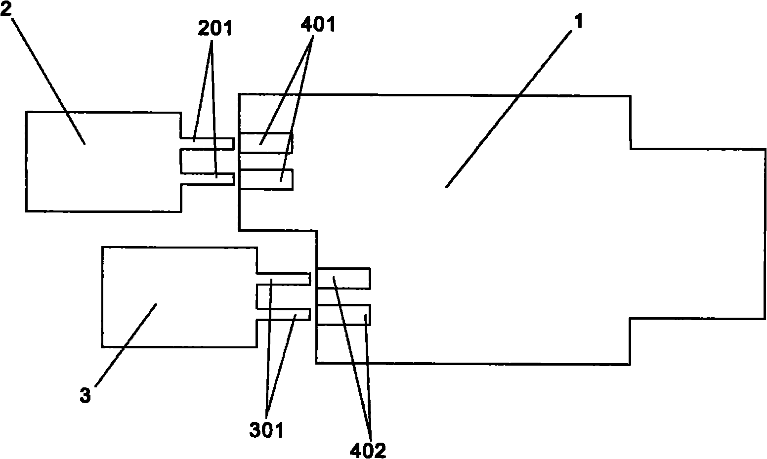
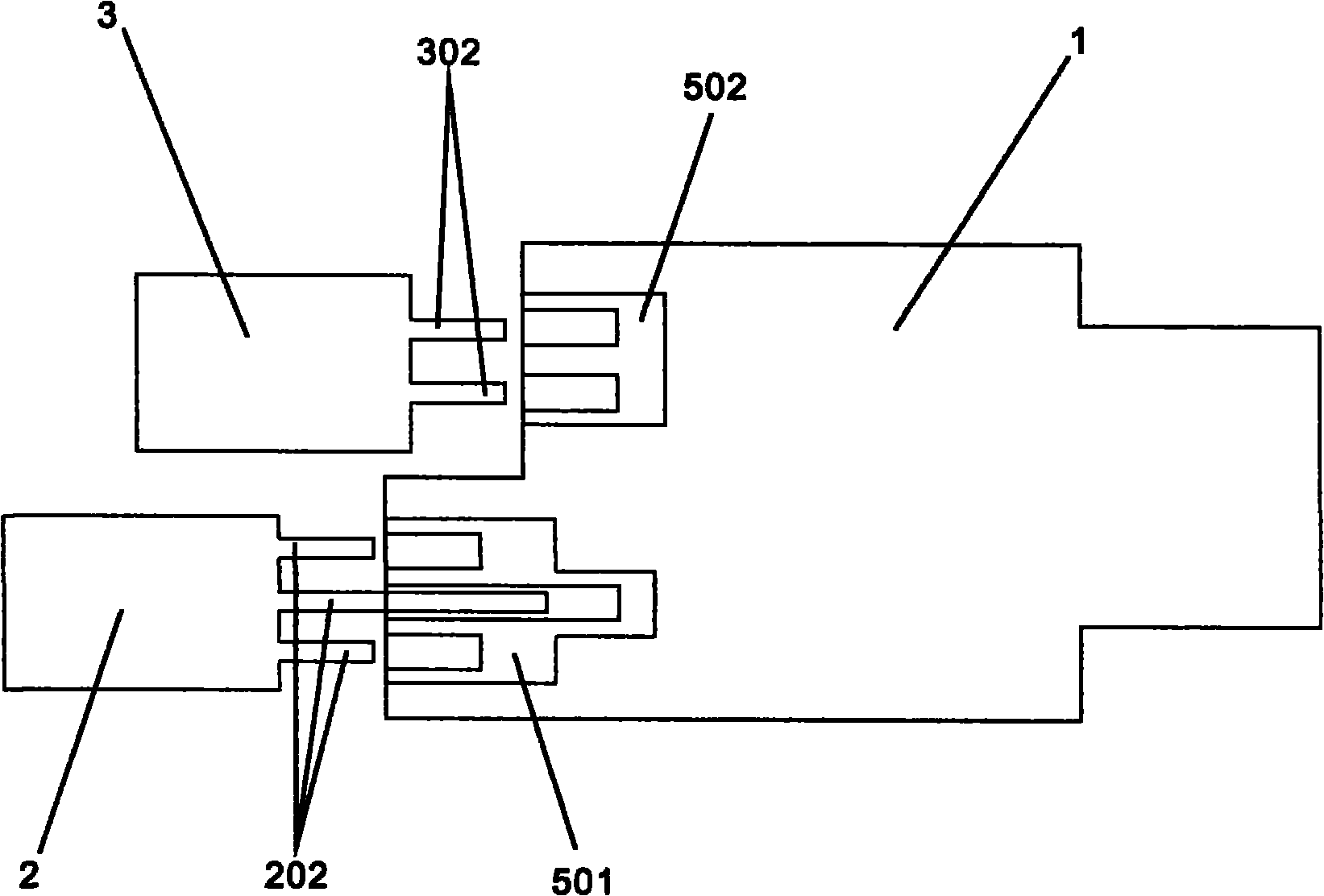
[0026] figure 1 It is a bottom view of the connection device between the optical transceiver device and the printed circuit board in the specific embodiment of the present invention. Optical transceiver devices include light receiving devices and light emitting devices. Such as figure 1 As shown, a strip-shaped metallized groove 401 is provided at the position where the bottom layer of the printed circuit board 1 of the pluggable optoelectronic module interferes with the lower side pin 201 of the light receiving device 2, and the metallized groove 401 is used for soldering the light receiving device. The lower side pins of the device. A strip-shaped metallization groove 402 is provided at the position where the bottom layer of the printed circuit board interferes with the lower side pins 301 of t...


PUM


Abstract

The invention discloses a method and a device for connecting an optical transceiving device with a printed circuit board (PCB), and is applicable to a pluggable photoelectric module. The method comprises the following steps of arranging a metalized groove on the position where the bottom layer of the PCB is interfered with a pin mounted at the lower side of the optical transceiving device; manufacturing a connecting plate for connecting the optical transceiving device and the PCB; when the connecting plate is connected with the top layer of the PCB, the distance between a bonding pad of the connecting plate and the metalized groove of the PCB is equal to that of the pin mounted at the upper side of the optical transceiving device and the pin mounted at the lower side of the optical transceiving device; the connecting plate is welded on the top layer of the PCB; the pin mounted on the upper side of the optical transceiving device is correspondingly welded with the bonding pad of the connecting plate; the pin mounted at the lower side of the optical transceiving device is correspondingly welded with the metalized groove of the PCB. By adopting the technical scheme in the invention, clubfoot shaping for the optical transceiving device can be avoided, the optical transceiving device is not damaged easily, the operation is simple and the connection is reliable.

Description

technical field [0001] The invention relates to the technical field of pluggable photoelectric modules, in particular to a method and device for connecting an optical transceiver and a printed circuit board. Background technique [0002] The pluggable photoelectric module is a standardized product widely used in optical communication systems to realize photoelectric conversion. The pin definition, structural size and other parameters of this type of product are stipulated by the multi-protocol developed by the multi-protocol committee for miniaturized transceivers (such as: SFP MSA). The position of the golden finger of the main printed board of the pluggable optoelectronic module and the position of the optical axis of the optical transceiver device are stipulated in the multiple agreement, but due to the plane of the golden finger of the main printed board of the pluggable optoelectronic module and the optical axis of the optical transceiver device The horizontal planes a...

Claims


Application Information

Patent Timeline
Patent Type & Authority Patents(China)
IPC IPC(8): H05K3/34H05K1/18
Inventor 曾雪飞杨忠熊磊邹渊周庭铭
Owner CHENGDU SUPERXON COMM TECH CO LTD
Why Eureka
Try Eureka