Method for producing light-emitting device

A technology for a light-emitting device and a manufacturing method, which is applied to the lighting device, the parts of the lighting device, and the cooling/heating device of the lighting device, etc. problem, to achieve the effect of suppressing color deviation

Inactive Publication Date: 2010-01-27
SHARP KK
View PDF3 Cites 9 Cited by
  • Summary
  • Abstract
  • Description
  • Claims
  • Application Information

AI Technical Summary

Problems solved by technology

[0007] Therefore, when the sealing resin is a thermosetting resin such as silicone resin and the temperature of the flow path portion is relatively high, the fluorescent body sinks while the sealing resin stagnates in the flow path portion in a low-viscosity state, causing its Uniform dispersion is destroyed
In addition, due to the variation in curing time, the degree of sinking of the phosphor also varies, so there is a problem of color variation in the emitted light.

Method used


Image

  • Method for producing light-emitting device
  • Method for producing light-emitting device
  • Method for producing light-emitting device

Examples


Embodiment approach 1

[0044] (light emitting device)

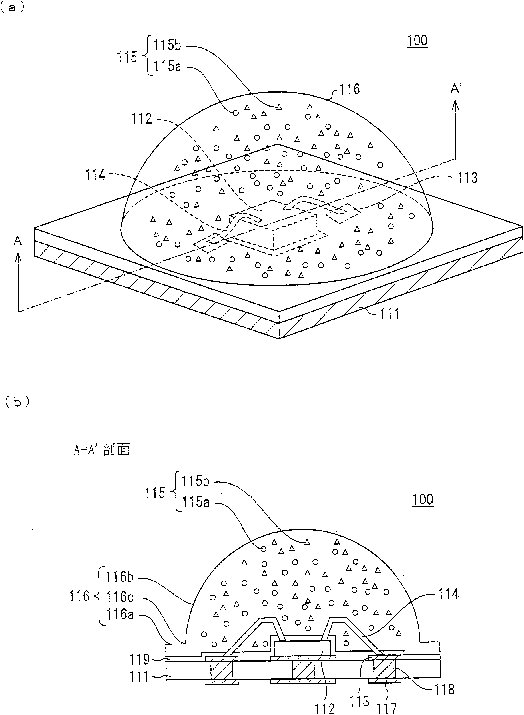
[0045] figure 1 It is an external view of the light emitting device according to the first embodiment of the present invention. The light emitting device 100 has a substrate 111 , a chip 112 mounted on the substrate 111 , leads 114 for connecting the chip 112 and wiring 113 , and a sealing resin 116 . The substrate 111 is, for example, a square with a length and width of 3.2 mm and a thickness of 0.6 mm; the sealing resin 116 covers the chip 112 , wiring 113 , leads 114 and the substrate 111 . The sealing resin 116 is used as a wavelength conversion part, and the fluorescent substance 115 is previously dispersed in the inside.

[0046] In the following description, the wavelength converting portion or the phosphor-containing resin, peripheral layer, and transparent resin described later will be appropriately rephrased as sealing resin.

[0047] The sealing resin 116 has a flat portion 116 a arranged to overlap the substrate and a hemispheric...

Embodiment approach 2

[0093] Figure 6 It is an external view of a light emitting device according to a second embodiment of the present invention. In this embodiment, a light-emitting device is manufactured by the same method as in the first embodiment, the wavelength conversion portion 216 of the light-emitting device is covered with a transparent peripheral layer 121, and the peripheral layer 121 is formed by secondary molding of a transparent resin.

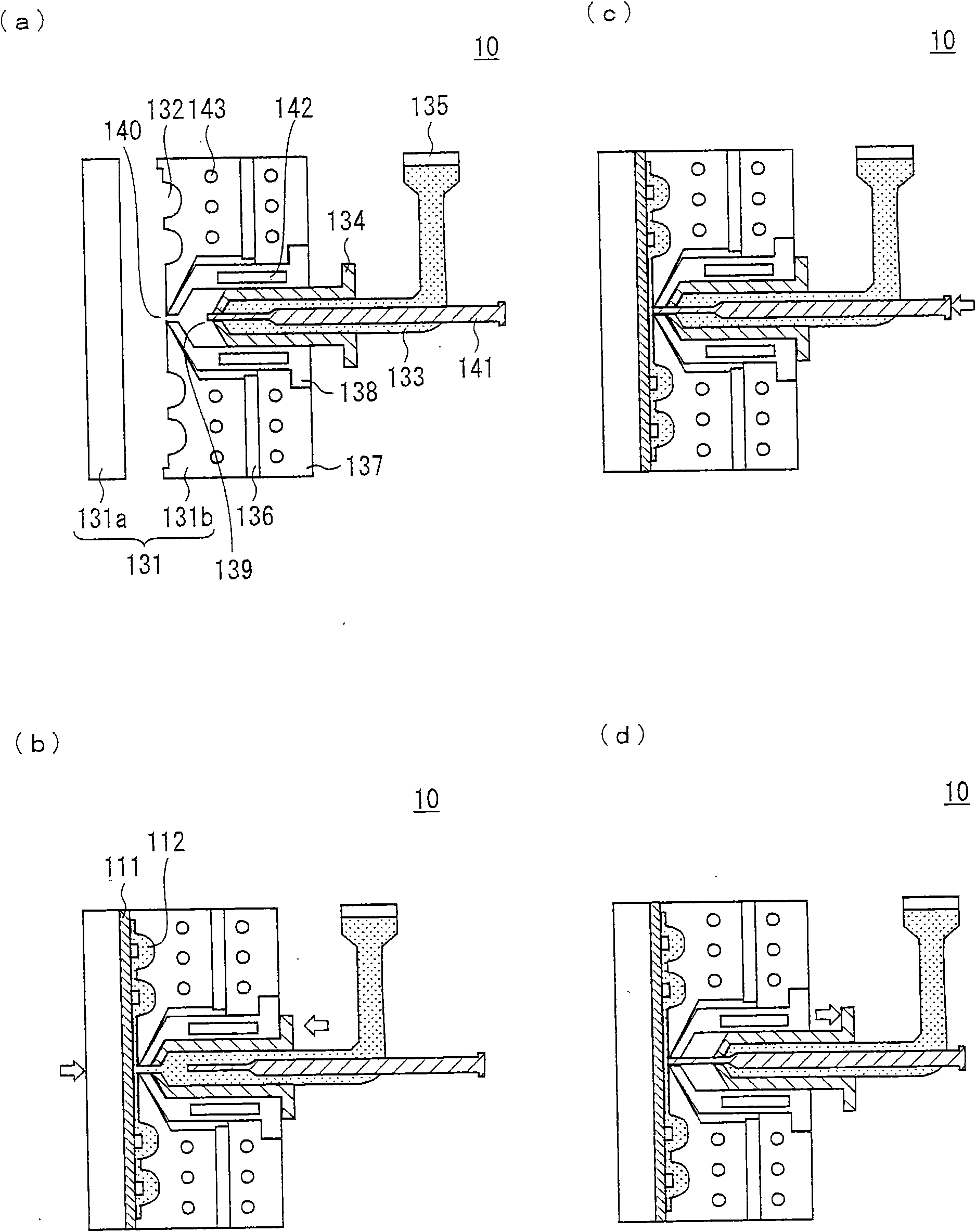
[0094] In the following description, the process from setting the substrate to taking out the molded product described in Embodiment 1 is referred to as primary molding, and a molded product formed by the primary molding is referred to as a primary molded product. The process of covering the peripheral layer 121 with the wavelength converting portion 216 formed in the primary molding (that is, the process from setting the substrate to taking out the molded product) is called secondary molding.

[0095] Hereinafter, the structure and manufacturing...

Embodiment approach 3

[0105] Figure 8 It is an external view showing a light emitting device according to a third embodiment of the present invention. This embodiment is characterized in that a rough portion 122 or a recessed portion 123 is formed in advance on the surface of the substrate 111 on which the chip 112 is mounted, and a part of the sealing resin 316 is embedded in the rough portion 122 or the recessed portion 123 . Therefore, the sealing resin 316 and the substrate 111 are more firmly bonded by the anchoring effect.

[0106] According to this embodiment, the sealing resin 316 is directly bonded to the substrate 111 without applying a primer. Of course, a primer can also be applied. In addition, the recessed portion 123 may penetrate the substrate 111 or may not penetrate the substrate 111 .

[0107] Regarding the method of forming the rough portion 122 or the depressed portion 123 on the substrate 111, for example, in the manufacturing process of the substrate 111, corresponding to...


PUM

PropertyMeasurementUnit
Diameteraaaaaaaaaa

Abstract

To restrain color variation in light emitted from a light-emitting device. A method for producing a light-emitting device includes the steps of: (a) die-bonding a chip onto a substrate so as to prepare a die-bonded substrate; (b) preparing a mold having a cavity; (c) setting the die-bonded substrate such that the chip is placed in the cavity; and (d) injecting sealing resin into the cavity via a runner section. In the method, the runner section is capable of maintaining its temperature at a low temperature lower than a temperature of the mold and the step (d) injecting the sealing resin that is maintained at the low temperature in the runner section, into the cavity via the runner section.

Description

technical field [0001] The invention relates to a manufacturing method of a light-emitting device sealed by resin. Background technique [0002] Currently, Patent Document 1 (Japanese Patent Application Laid-Open Publication No. 2007-332259; published on December 27, 2007) discloses a method for manufacturing a light-emitting device having a light-emitting element that emits blue light ( Chip) and the phosphor that emits fluorescence after absorbing the blue light of the light-emitting element, and white light is obtained according to the blue light of the light-emitting element and the fluorescence of the phosphor. In this manufacturing method, a resin sheet is formed of a curable silicone resin composition containing a phosphor, and the resin sheet is transfer-molded to cover the chip, and the transfer-molded resin is used as a wavelength converting portion. [0003] In addition, regarding a molding method of a thermosetting resin, Patent Document 2 (Japanese Patent Appli...

Claims


Application Information

Patent Timeline
IPC IPC(8): H01L33/00F21V19/00F21V29/00F21V9/10F21Y101/02F21V9/40
CPCB29K2083/00H01L2933/005B29C45/14655H01L33/52H01L33/504H01L2933/0041B29C45/2756H01L2224/48227B29K2101/10H01L2224/48235H01L2224/8592H01L2924/181H01L2924/00012
Inventor 小西正宏太田将之冈田丰稻田顺史
Owner SHARP KK
Why Eureka
Try Eureka