
Method for optimizing area of mixed signal chip

A chip area, mixed signal technology, applied in special data processing applications, instruments, electrical digital data processing, etc., can solve the problems of large IP area, large chip area, large device area, etc., to optimize performance and reduce chip area , the effect of reducing the use of capacitors or resistors

Active Publication Date: 2010-03-17
BEIJING TONGFANG MICROELECTRONICS
View PDF0 Cites 9 Cited by
  • Summary
  • Abstract
  • Description
  • Claims
  • Application Information

AI Technical Summary

Problems solved by technology

The problem caused by this method is: in the well-made IP that is usually used, such as regulator (level shifter) or chargepump (charge pump), there are a large number of capacitors and resistors.
And these devices often occupy a larger area, which will make the completed IP area larger
When the chip is laid out, the size and area of ​​the IP are fixed, and some wasteful areas will be generated on the chip, resulting in a larger chip area
At the same time, devices such as capacitors or resistors in the IP are simulated separately from the chip, so the number of capacitors or resistors installed in this way is often greater than the actual needs of the chip

Method used


Image

  • Method for optimizing area of mixed signal chip
  • Method for optimizing area of mixed signal chip
  • Method for optimizing area of mixed signal chip

Examples


Embodiment 1

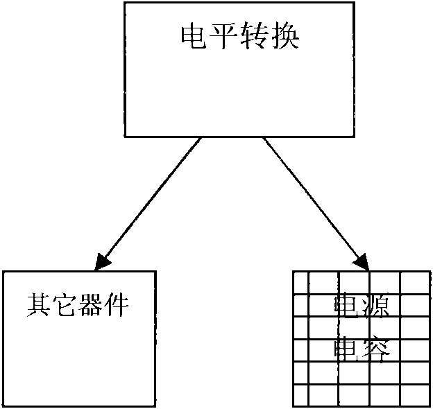
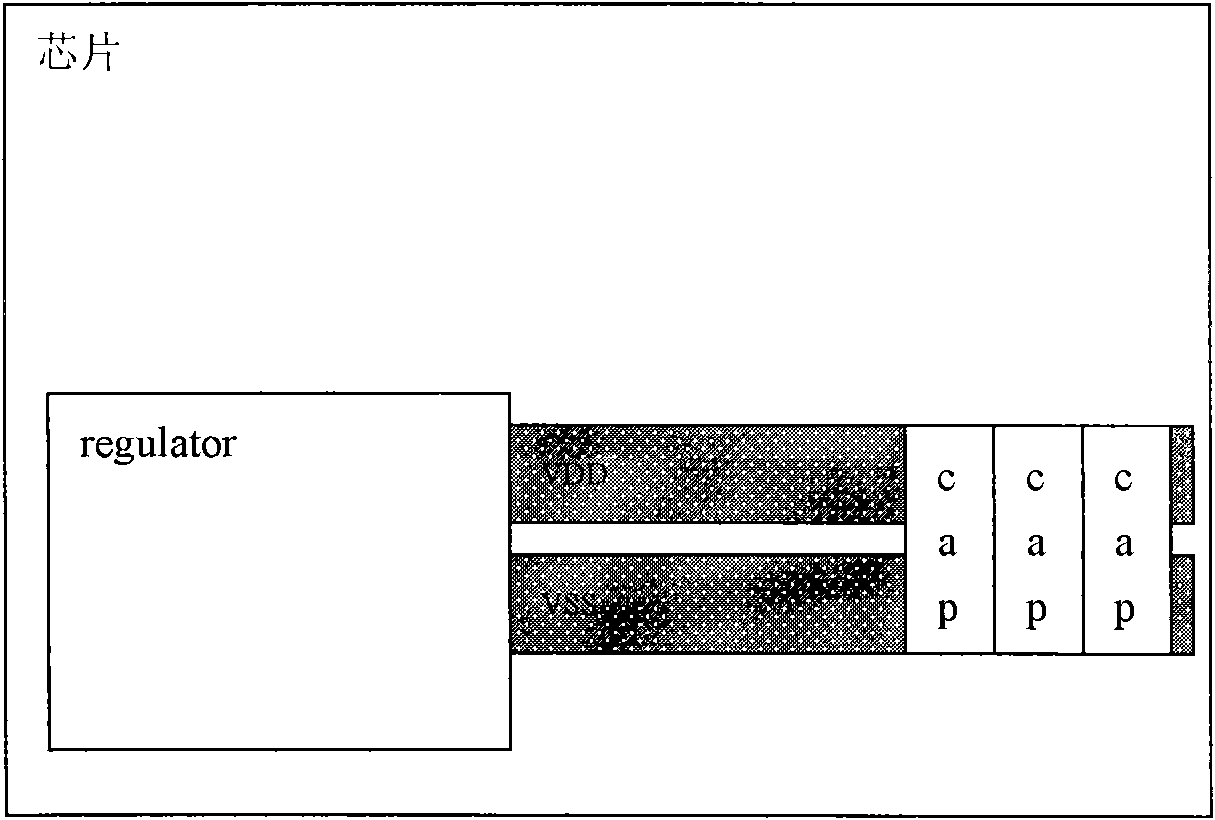
[0023] see Figure 1 to Figure 3 , the steps of the method for optimizing the area of ​​the mixed-signal chip in the present invention are:

[0024] ① When designing the regulator layout, separate the capacitors in the regulator to greatly reduce the area of ​​the regulator;

[0025] ② Arrange the completed regulator and other logic units to obtain the area of ​​the entire chip;

[0026] ③ Place the separated capacitor on the power ring on the chip or under the pad that uses a different metal layer from the capacitor.

Embodiment 2

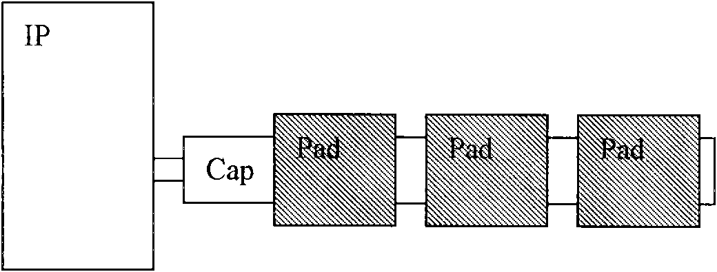
[0028] A method for optimizing the area of ​​a mixed-signal chip is as follows:

[0029] ① When designing the IP layout, do not place resistors or capacitors in the IP, so that the IP area is greatly reduced;

[0030] ② Arrange the completed IP and other logic units to obtain the area of ​​the entire chip;

[0031] ③ According to the simulation of the whole chip, the number of resistors or capacitors to be added is obtained, and the resistors or capacitors are placed on the chip power ring, under the pad pad, or in a wiring area that is different from the metal layer used by the resistors or capacitors .


PUM


Abstract

The invention discloses a method for optimizing the area of a mixed signal chip, which relates to the technical field of integrated circuit. The method of the invention comprises the following steps:(1) when designing an IP layout, separating resistors or capacitors out of the IP to reduce the IP area substantially; (2) arranging the prepared IP and other logic units to obtain the area of the whole chip; and (3) placing the resistors or the capacitors which are separated out on a chip power ring, under a pad or in a wiring area which is different from the metal layer used by the resistors orthe capacitors. Compared with the prior art, the invention ensures the IP performance and simultaneously reduces the IP area, further optimizes the chip area, does not generate a waste area, and savesthe numbers of the resistors and the capacitors.

Description

technical field [0001] The invention relates to the technical field of integrated circuits, in particular to a method for optimizing the area of ​​mixed-signal chips. Background technique [0002] At present, the digital layout method of an integrated circuit is to arrange the completed IP (module), IO (input and output) and logic units, so as to obtain the area of ​​the entire chip. The problem caused by this method is that there are a large number of capacitors and resistors in the well-made IP that is usually used, such as regulator (level shifter) or chargepump (charge pump). And these devices often occupy a larger area, which will make the completed IP area larger. When the chip is laid out, the size and area of ​​the IP are fixed, which will generate some wasted areas on the chip, resulting in a larger chip area. At the same time, devices such as capacitors or resistors in the IP are simulated separately from the chip, so the number of capacitors or resistors install...

Claims


Application Information

Patent Timeline
IPC IPC(8): G06F17/50
Inventor 孙喆王磊侯晓宇李婧娴祁寒侯艳梁天逾张云翔
Owner BEIJING TONGFANG MICROELECTRONICS
Learn More