Semiconductor chip module

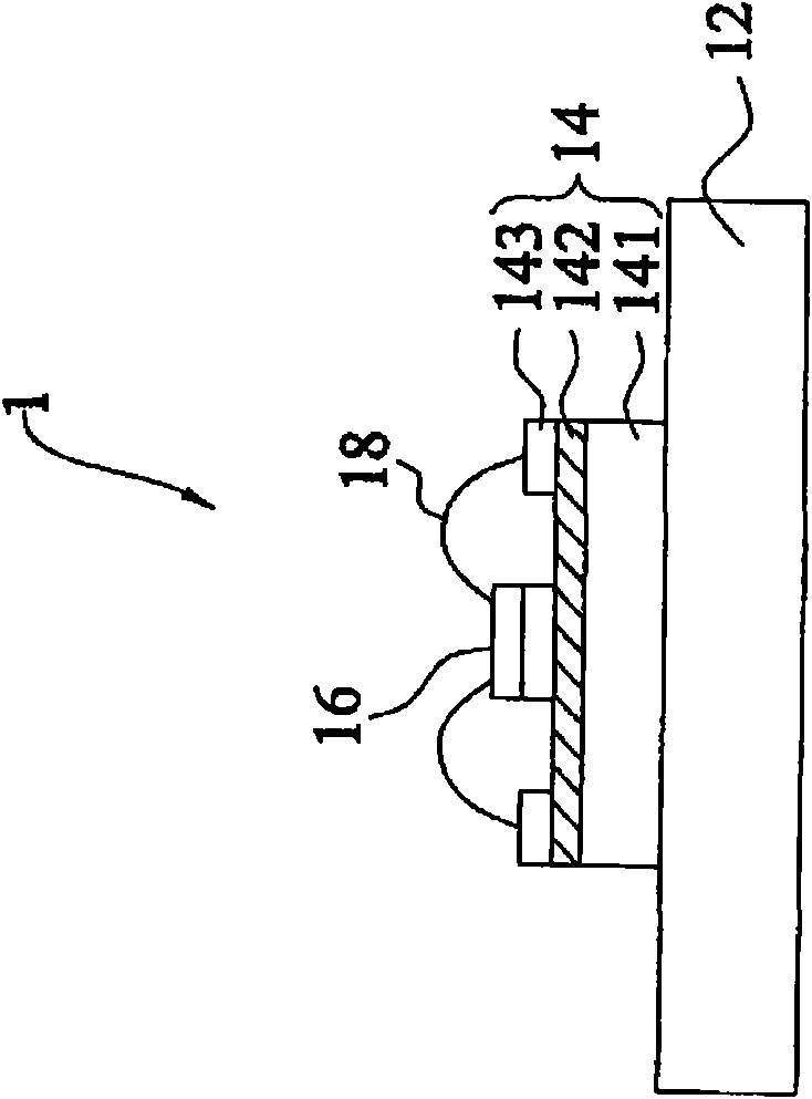
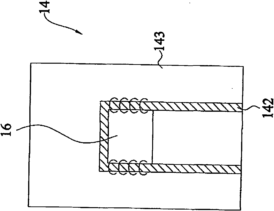
A chip module and semiconductor technology, which is applied to semiconductor devices, semiconductor/solid-state device components, electric solid-state devices, etc., can solve the problems of poor heat dissipation efficiency, poor efficiency of the base 12, and high manufacturing cost of the solar chip module 1, and saves energy. The effect of manufacturing cost and improving heat dissipation efficiency

Inactive Publication Date: 2010-03-31
SOLAPOINT CORP
View PDF0 Cites 0 Cited by
  • Summary
  • Abstract
  • Description
  • Claims
  • Application Information

AI Technical Summary

Problems solved by technology

[0006] The heat transferred to the base 12 through the insulating layer 142, because the insulating layer 142 is generally thicker, the heat dissipation efficiency is poor, so the efficiency of heat transfer to the base 12 is very poor
[0007] The cost of materials for making the substrate 14 is high, so the cost of making the solar chip module 1 is very high

Method used


Image

  • Semiconductor chip module
  • Semiconductor chip module
  • Semiconductor chip module

Examples


Embodiment Construction

[0059] In order to further understand the purpose, structure, features, and functions of the present invention, the detailed description of the accompanying examples is as follows.

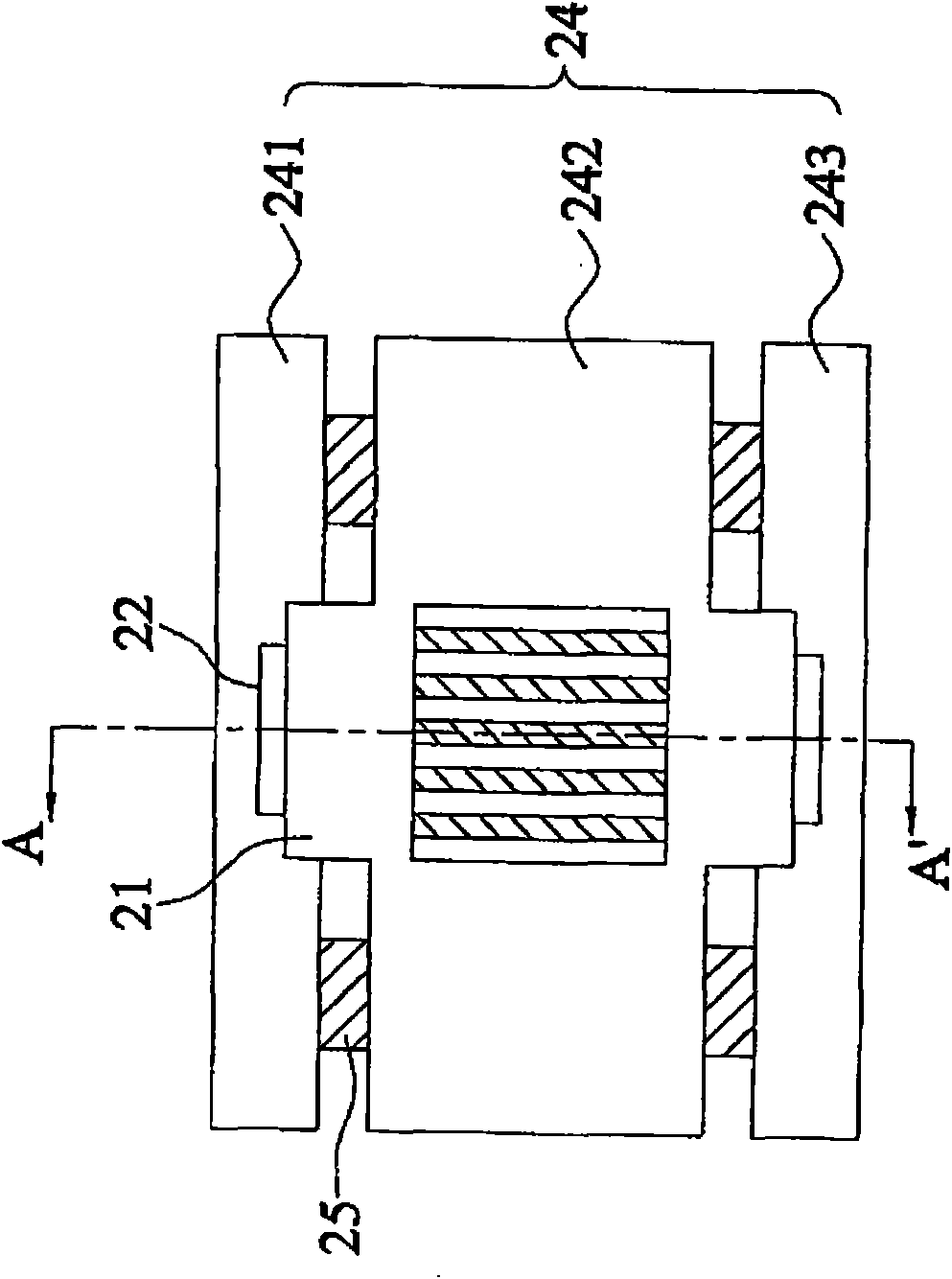
[0060] Figure 2A A top view of the semiconductor chip module 2 of the present invention is shown according to the first embodiment. Figure 2B for the semiconductor chip module 2 along the Figure 2A A cross-sectional view of the dotted line A-A'. image 3 It is an exploded view of the structure of the conductive frame 21 , the flexible cable 22 and the semiconductor chip 23 of the semiconductor chip module 2 .

[0061] As shown in the figure, the semiconductor chip module 2 includes a conductive frame 21 , a flexible cable 22 , a semiconductor chip 23 and a heat dissipation structure 24 . The semiconductor chip 23 defines a front side 23a and a back side 23b. The semiconductor chip 23 has a first electrode 231 and a second electrode 232 located on the front side 23a and the back side 23b res...


PUM


Abstract

The invention provides a semiconductor chip module comprising a conducting frame, a flexible flat cable, a semiconductor chip and a heat radiation structure, wherein the conducting frame is provided with an inner edge and an outer edge, and the inner edge defines an opening; the flexible flat cable is provided with a conductor layer electrically connected with the outer edge of the conducting frame; the semiconductor chip defines a front side and a back side and is provided with a first electrode and a second electrode which are respectively positioned on the front side and the back side, thefirst electrode is connected with the inner edge of the conducting frame so that the semiconductor chip is positioned below the conducting frame, and the semiconductor chip is exposed in the opening;and the heat radiation structure bears the semiconductor chip and directly contacts the second electrode to enhance the heat radiation efficiency of the semiconductor chip.

Description

technical field [0001] The invention relates to a semiconductor chip module, in particular to a semiconductor chip module in which the electrodes of the semiconductor chip directly contact the heat dissipation structure. Background technique [0002] Figure 1A Show the side view of known solar chip module 1; Figure 1B A top view of a known solar chip 16 on a substrate 14 is shown. Such as Figure 1A and 1B As shown, the solar chip module 1 includes a base 12 ; a substrate 14 placed on the base 12 and a solar chip 16 placed on the substrate 14 . [0003] The substrate 14 is sequentially formed by stacking the metal layer 141 , the insulating layer 142 and the conductive contact 143 , and the conductive contact 143 does not completely cover the insulating layer 142 . The solar chip 16 is placed on the insulating layer 142 and has a gap with the conductive contact 143 . The solar chip module 1 utilizes the lead wire 18 to electrically connect the solar chip 16 to the cond...

Claims


Application Information

Patent Timeline
Patent Type & Authority Applications(China)
IPC IPC(8): H01L23/367H01L31/052H01L31/024
CPCH01L2924/0002Y02E10/50
Inventor 刘台徽
Owner SOLAPOINT CORP
Why Eureka
Try Eureka