

Memory controller
A memory controller and memory technology, applied in the computer field, can solve the problems of inflexible memory controller configuration and high memory update costs, and achieve the effects of reducing implementation costs, improving flexibility, and reducing costs
- Summary
- Abstract
- Description
- Claims
- Application Information
AI Technical Summary
Problems solved by technology
Method used
Image

Examples
Embodiment Construction
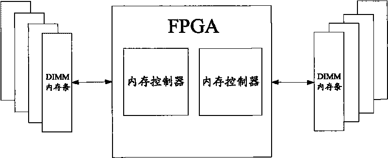
[0024] Aiming at the problem in the related art that the configuration of the memory controller is not flexible enough to cause high cost of memory update, the present invention proposes to implement the memory controller through a Field Programmable Gate Array (Field Programmable Gate Array, referred to as FPGA), thereby controlling the memory, Because the FPGA itself has strong configurability, it can adapt to the configuration update of the memory, and can also manage multiple memory sticks at the same time, effectively improving the flexibility of the design.
[0025] Embodiments of the present invention will be described in detail below with reference to the accompanying drawings.
[0026] In an embodiment of the present invention, a memory controller is provided. The memory controller according to the present invention can be realized based on FPGA.
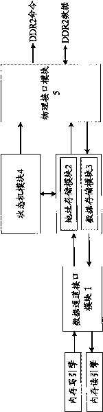
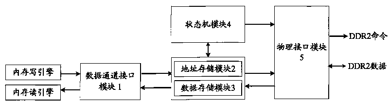
[0027] Such as figure 1 As shown, the memory controller according to the embodiment of the present invention includes: ...
PUM
 Abstract
Description
Claims
Application Information