Two-way blocking-up type surge protection device
A technology of surge protection devices and resistors, which is applied in the direction of automatic disconnection emergency protection devices, emergency protection circuit devices, and protection against overvoltages, etc., which can solve the problems of inability to give the system security, repair of damaged equipment, and reduction in productivity, etc. problems, to achieve the effect of easy protection design, improved performance, and low unit cost
- Summary
- Abstract
- Description
- Claims
- Application Information
AI Technical Summary
Problems solved by technology
Method used
Image
Examples
Embodiment 1
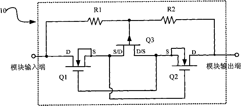
[0041] see figure 1 As shown in the schematic diagram of the circuit structure of Embodiment 1 of the present invention, a bidirectional blocking surge protection device 10 is composed of a first depletion type field effect transistor Q1 (a depletion type N-channel metal oxide semiconductor field effect transistor NMOSFET), the second depletion type field effect transistor Q2 (depletion type N-channel metal oxide semiconductor field effect transistor NMOSFET), the third depletion type field effect transistor Q3 (depletion type P-channel junction field effect transistor PJFET) and a variable resistor circuit module composed of the first resistor R1 (constant current source resistor) and the second resistor R2 (constant current source resistor).
[0042] The connection relationship of each device inside the surge protection device 10 (BSP) is described as follows: the source S of the first depletion type field effect transistor Q1 of the bidirectional blocking type surge protect...
Embodiment 2
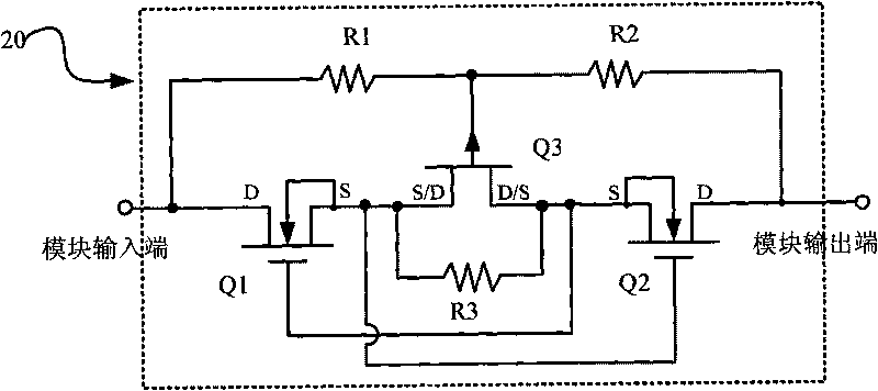
[0048] see figure 2 As shown in the schematic diagram of the circuit structure of Embodiment 2 of the present invention, as an improvement on the surge protection device of Embodiment 1, a third resistor R3 (bias resistor) is added to the surge protection device 20, and the third resistor R3 is connected in parallel Between the source S and the drain D of the third depletion-type field effect transistor Q3, that is, the third resistor R3 is connected to the source S of the first depletion-type N-channel field-effect transistor Q1 and the second depletion-type N-channel The source S of the field effect transistor Q2.
[0049] The third resistor R3 is the source S of the first depletion type field effect transistor Q1 or the second depletion type field effect transistor after any one of the first and second depletion type field effect transistors Q1 and Q2 is turned off The source S of Q2 provides a stable potential, preventing this node from floating in the "blocking" state o...
Embodiment 3
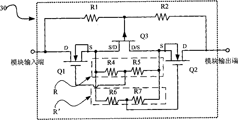
[0051] see image 3 As shown in the schematic diagram of the circuit structure of Embodiment 3 of the present invention, as an improvement on the surge protection device of Embodiment 1, the surge protection device 30 adds a first feedback voltage divider R and a second feedback voltage divider R ', the first feedback voltage divider R is composed of the fourth resistor R4 and the fifth resistor R5, the fourth resistor R4 and the fifth resistor R5 of the first feedback voltage divider R are connected in parallel to the third depletion type field effect transistor Q3 Between the drain D and the source S, the middle node of the first feedback voltage divider R is connected to the gate G of the first depletion type field effect transistor Q1; the second feedback voltage divider R' is connected by the sixth resistor R6 and the seventh resistor R7, the second feedback voltage divider R' is connected in parallel between the drain D and the source S of the third depletion-type field ...
PUM
 Abstract
Description
Claims
Application Information


