Semiconductor laser device

A laser device and semiconductor technology, applied in the direction of semiconductor lasers, lasers, laser components, etc., can solve problems such as the loss of the effect of the tapered structure, achieve the effect of suppressing complexity and realizing high temperature and high power operation

Active Publication Date: 2010-05-26
SHARP FUKUYAMA LASER CO LTD
View PDF5 Cites 13 Cited by
  • Summary
  • Abstract
  • Description
  • Claims
  • Application Information

AI Technical Summary

Problems solved by technology

In other words, the situation is closer to the case of constant bar width, resulting in a loss of the effect of the tapered structure

Method used


Image

  • Semiconductor laser device
  • Semiconductor laser device
  • Semiconductor laser device

Examples


no. 1 example

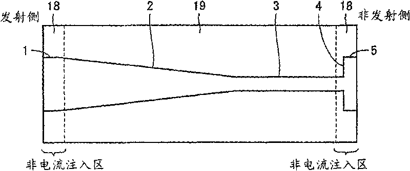
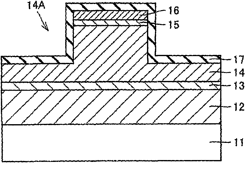
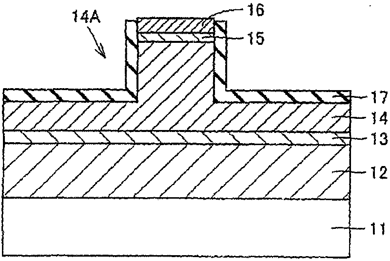
[0060] figure 2 The cross-sectional view of is showing the cross-section of the window region 18 in the semiconductor laser device according to the first embodiment of the present invention. image 3 The cross-sectional view of is showing the cross-section of the inner region 19 in the semiconductor laser device.

[0061] Such as figure 2 and 3 As shown, the semiconductor laser device according to the present embodiment has a laminated structure formed continuously above the n-type GaAs substrate 11, the laminated structure at least includes: n-type AlGaInP cladding layer 12; multi-quantum well active layer 13, including Non-doped AlGaInP optical guide layer, non-doped GaInP well layer and non-doped AlGaInP barrier layer; p-type AlGaInP cladding layer 14; p-type GaInP discontinuous relaxation layer 15; and p-type GaAs capping layer 16. In the window area 18 set near the end face of the resonator ( figure 2 ) diffuses zinc (Zn) to thereby disorder the multi-quantum well ...

no. 2 example

[0082] Figure 12A and 12B The schematic diagrams of are each showing a cross section of the semiconductor laser device according to the second embodiment. Figure 12A shows a cross-section of the inner region 19, while Figure 12B A cross-section of the window region 18 is shown.

[0083] This semiconductor laser device is a modification of the semiconductor laser device according to the first embodiment, and is characterized in that the multi-quantum well active layer includes GaAs and AlGaAs, and the semiconductor laser device is a CD-R high-power infrared laser device having a 780 nm energy The oscillation wavelength of the band.

[0084] refer to Figure 12A and 12B , the semiconductor laser device according to the present embodiment has a structure in which stacked layers are continuously formed over the n-type GaAs substrate 21 . The stacked structure consists of at least n-type AlGaInP cladding layer 22; multi-quantum well active layer 23 including non-doped AlGa...

no. 3 example

[0092] Figure 13A and 13B The schematic diagrams of are each showing a cross section of the semiconductor laser device according to the third embodiment. Figure 13A shows a cross-section of the inner region 19, while Figure 13B A cross-section of the window region 18 is shown.

[0093] This semiconductor laser device is a modification of the semiconductor laser device according to the first and second embodiments, characterized in that the structure of the multi-quantum well active layer includes GaN and InGaN, and the semiconductor laser device is a high-power infrared laser device of BD, Oscillation wavelength with 405nm energy band.

[0094] refer to Figure 13A and 13B , the semiconductor laser device according to the present embodiment has a structure in which stacked layers are continuously formed over the n-type GaN substrate 31 . The stacked structure is at least composed of an n-type AlGaN cladding layer 32; a multi-quantum well active layer 33 including a Ga...


PUM


Abstract

A resonator (100) in a semiconductor laser device includes a semiconductor substrate (11), an n-type cladding layer (12) and a p-type cladding layer (14) formed on or above the semiconductor substrate (11), and an active layer (13) sandwiched between the n-type cladding layer (12) and the p-type cladding layer (14). A ridge (14A) extending in an axial direction of the resonator (100) is formed at an upper surface of the resonator (100). The ridge (14A) includes an emitting-side end portion (1), a non-emitting-side end portion (5), a taper portion (2) allowing a width of the ridge (14A) to be decreased in a taper-like manner from the emitting-side end portion (1) toward the non-emitting-side end portion (5), and a step portion (4) provided on a side of the emitting-side end portion (1) with respect to the non-emitting-side end portion (5), and allowing the width of the ridge to be changed in a step-like manner.

Description

technical field [0001] The present invention relates to semiconductor laser devices, and in particular, to semiconductor laser devices used in optical pickup devices and other devices. Background technique [0002] In recent years, recording speeds have been improved on optical pickup devices. For example, CD-R, DVD-R / RW, and other devices realizing a 16X recording speed have been commercialized. In order to increase the recording speed, semiconductor laser devices need to achieve high power. [0003] In order to achieve high power semiconductor laser devices, it is required: high COD (Catastrophic Optical Damage-catastrophic optical damage) level, that is, high optical power limit determined by COD; linearity in current-optical power characteristics, that is, high kink level ( high kink level); and low operating current at high temperature operation, etc. [0004] In order to improve the COD level, for example, as shown in Japanese Laid-Open Publication No. 2001-015864, ...

Claims


Application Information

Patent Timeline
Patent Type & Authority Applications(China)
IPC IPC(8): H01S5/343H01S5/16
CPCH01S5/1039H01S5/162H01S5/0655H01S5/10H01S5/32341H01S5/34326H01S5/16H01S5/1064B82Y20/00
Inventor 菅原章义
Owner SHARP FUKUYAMA LASER CO LTD
Why Eureka
Try Eureka