Decoding method of power supply line of memory array

A memory and memory cell technology, applied in static memory, digital memory information, information storage, etc., can solve the problems of high power, consumption, and difficulty in reducing device power consumption, and achieve the goal of reducing standby current, simple design, and low-cost implementation. Effect

Active Publication Date: 2010-06-09
SEMICON MFG INT (SHANGHAI) CORP +1
View PDF0 Cites 11 Cited by
  • Summary
  • Abstract
  • Description
  • Claims
  • Application Information

AI Technical Summary

Problems solved by technology

Although fabless chip companies and foundry services have increased in recent years, many limitations remain
For example, leakage currents in memory devices make it difficult to reduce overall device power consumption due to scaling of logic devices and designs operating at low voltages
Memory devices such as static random access memory (SRAM) consume large amounts of power in many integrated circuit applications

Method used


Image

  • Decoding method of power supply line of memory array
  • Decoding method of power supply line of memory array
  • Decoding method of power supply line of memory array

Examples


Embodiment Construction

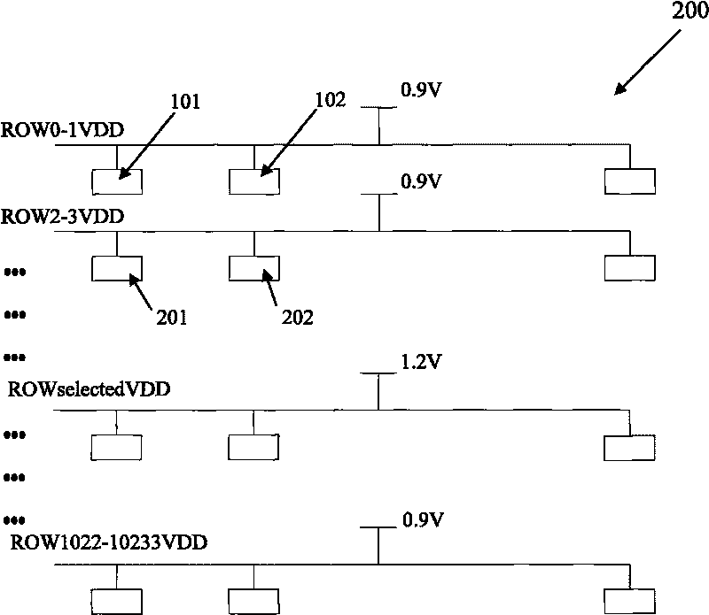
[0025] According to the present invention, an integrated circuit and a process thereof for semiconductor device manufacture are provided. More specifically, the present invention provides a method and apparatus for selectively reducing the supply voltage of an SRAM memory array. By way of example only, the invention has been applied to SRAM devices to provide low power consumption while maintaining high storage speeds. It should be realized, however, that the invention has a much wider range of applicability. For example, the invention is applicable to other embedded or stand-alone integrated circuit memories, such as DRAM and non-volatile memories.

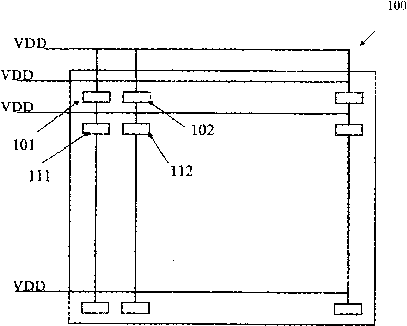
[0026] figure 1 is a schematic diagram of an existing SRAM array 100 . As shown, the SRAM memory array 100 includes memory cells, such as 101 , 102 , . . . , 111 , 112 . . . . In a typical existing SRAM array, such as the SRAM array 100, all memory cells are supplied with the same power supply voltage VDD. The power grid in ...


PUM


Abstract

The invention provides a decoding method of a power supply line of a memory array, which is a method for selectively supplying voltage supply in an integrated circuit memory device. In the method, an integrated circuit device is provided and comprises multiple first memory units; each memory unit comprises a power supply terminal and a grounding terminal; multiple second memory unit are selected from the multiple first memory units; a first power supply voltage is supplied to the power supply terminal of each memory unit selected, and a second power supply voltage is supplied to the power supply terminal of each unselected memory unit; and the second power supply voltage is lower than the first power supply voltage. In an embodiment of the method, a first grounding voltage is applied to the grounding terminal of each selected memory unit, a second grounding voltage is applied to the grounding terminal of each unselected memory unit, and the second grounding voltage is higher than the first grounding voltage.

Description

technical field [0001] The present invention relates to a memory device and a method for providing a voltage supply thereof Background technique [0002] Integrated circuits, or "ICs," have grown from a handful of interconnected devices fabricated on a single chip of silicon to millions of devices. Existing ICs offer performance and complexity far beyond what was originally imagined. To achieve increases in complexity and circuit density (ie, the number of devices that can be packed onto a given chip area), the size of the smallest device feature, also referred to as device "geometry," has shrunk with each IC generation. Semiconductor devices are now being fabricated with feature sizes smaller than 1 / 4 micron. [0003] Integrated circuits, or "ICs," have grown from a handful of interconnected devices fabricated on a single chip of silicon to millions of devices. Existing ICs offer performance and complexity far beyond what was originally imagined. To achieve increases in...

Claims


Application Information

Patent Timeline
Patent Type & Authority Applications(China)
IPC IPC(8): G11C5/14G11C11/413
CPCG11C11/413G11C11/412G11C5/147
Inventor 欧阳雄李智黄强
Owner SEMICON MFG INT (SHANGHAI) CORP
Why Eureka
Try Eureka