Method for formlng pattern of semiconductor device

A semiconductor and pattern technology, applied in semiconductor devices, semiconductor/solid-state device manufacturing, electric solid-state devices, etc., can solve the problems of second photoresist pattern degradation profile, inability to properly perform follow-up procedures, etc., to ensure process margin, Effect of improving adhesion characteristics, reliable semiconductor devices

Inactive Publication Date: 2010-06-09
SK HYNIX INC
View PDF1 Cites 8 Cited by
  • Summary
  • Abstract
  • Description
  • Claims
  • Application Information

AI Technical Summary

Problems solved by technology

Therefore, the second photoresist pattern has a degraded profile
In addition, photoresist scum is generated between the spacer patterns, so that subsequent processes cannot be properly performed and the photoresist pattern is lifted due to adhesion defects between the substrate and the photoresist film.

Method used


Image

  • Method for formlng pattern of semiconductor device
  • Method for formlng pattern of semiconductor device
  • Method for formlng pattern of semiconductor device

Examples


Embodiment Construction

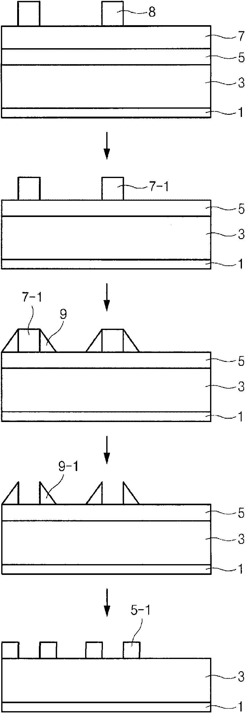
[0051] Figure 4a to Figure 4j is a view illustrating a method for forming a pattern of a semiconductor according to an embodiment of the present invention.

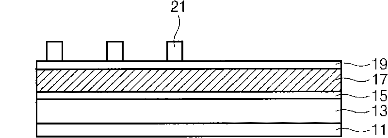
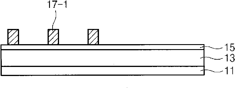
[0052] refer to Figure 4a , forming the base layer 111 on the substrate. The substrate may include an isolation film (ISO) (not shown), and the base layer 111 may include a dielectric film (not shown) [for example, an oxide film-nitride film-oxide film (ONO)], a gate polysilicon layer (not shown), a tungsten conductive layer (not shown), a capping oxide film (not shown), and a gate mask film (not shown).

[0053] A polysilicon layer 113, a first nitride film 115 (ie, a first mask film), an oxide film 117 (ie, a second mask film), and a third mask film 119 are sequentially deposited on the base layer.

[0054] The oxide film 117 is formed using tetraethyl silicate (TEOS). Since the oxide film 117 determines the spacer height in the spacer patterning process, it is required that the oxide film has a given height of ab...


PUM

PropertyMeasurementUnit
critical dimensionaaaaaaaaaa
widthaaaaaaaaaa

Abstract

A method for forming a pattern of a semiconductor device using a spacer patterning process comprises coating a developable antireflection film over a substrate including a spacer pattern, coating a photoresist film over the antireflection film, and patterning the antireflection film and the photoresist film by an exposing and developing process to form an etching mask pattern. The etching mask pattern has an excellent profile. When a lower underlying layer is etched using the etching mask pattern, a sufficient etching margin can be secured, thereby obtaining a reliable semiconductor device.

Description

technical field [0001] The present invention generally relates to methods of patterning semiconductor devices, and more particularly, to methods of patterning semiconductor devices such as NAND flash memory devices using spacer patterning techniques. Background technique [0002] In recent years, semiconductor technology has been rapidly developed to store an ever-increasing amount of information; to process or transmit information quickly; and to construct a simpler information communication network conforming to the information communication society of the 21st century. [0003] In particular, due to the rapid spread of information media such as computers, research has been conducted on the development of processing equipment or processing technology for manufacturing semiconductor devices. The purpose of the research is to produce smaller semiconductor components with higher capacity and lower manufacturing cost without degrading the electrical characteristics. [0004] ...

Claims


Application Information

Patent Timeline
Patent Type & Authority Applications(China)
IPC IPC(8): H01L21/82H01L21/8247H01L21/768G03F7/20
CPCH01L21/32139H01L27/11526H01L27/108H01L21/0337H01L27/11573H01L27/105H10B12/00H10B41/40H10B43/40H01L21/0276
Inventor 李基领
Owner SK HYNIX INC
Why Eureka
Try Eureka