Adhesive sheet for manufacturing semiconductor device, and semiconductor device manufacturing method using the sheet

A semiconductor and adhesive sheet technology, which is applied in the manufacture of semiconductor/solid-state devices, semiconductor devices, and components of semiconductor/solid-state devices, etc., can solve problems such as breakage and displacement of the mounting position of semiconductor wafers, so as to suppress the reduction of yield, Achieve bond precision, achieve downtime effects

Inactive Publication Date: 2010-06-30
NITTO DENKO CORP
View PDF3 Cites 10 Cited by
  • Summary
  • Abstract
  • Description
  • Claims
  • Application Information

AI Technical Summary

Problems solved by technology

In addition, even when a semiconductor chip is mounted, sometimes the mounting position of the semiconductor chip is shifted, and as a result, damage occurs due to contact with other semiconductor chips mounted at a predetermined position.

Method used


Image

  • Adhesive sheet for manufacturing semiconductor device, and semiconductor device manufacturing method using the sheet
  • Adhesive sheet for manufacturing semiconductor device, and semiconductor device manufacturing method using the sheet
  • Adhesive sheet for manufacturing semiconductor device, and semiconductor device manufacturing method using the sheet

Examples


Embodiment 1

[0093] First, an isocyanate-based crosslinking agent (Nippon Polyurethane Co., Ltd., trade name; Coronate HX) 3 parts, epoxy resin (made by Japan Epoxy Resin Co., Ltd., trade name; Epikote 1003) 33 parts, phenolic resin (Arakawa Chemical Co., Ltd., trade name; P-180) 22 parts and as pigment Dissolve 0.2 parts of ultrafine titanium oxide (manufactured by Titanium Industry Co., Ltd., trade name; STT-4D, average particle diameter: 0.15 μm) in methyl ethyl ketone, and stir to prepare a solution of an adhesive composition with a concentration of 15% by weight. .

[0094] The solution of the adhesive composition was ground and dispersed by a three-roll mill, centrifuged at 400 ppm, and filtered through a 0.7 μm glass filter.

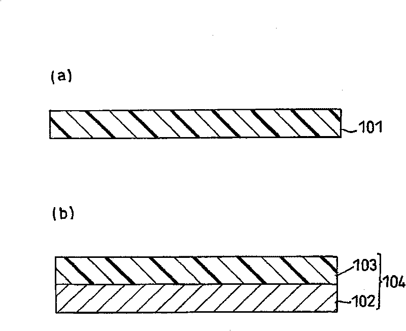
[0095] Next, the filtered solution of the adhesive composition was applied to a release-treated film (core material) containing a polyethylene terephthalate film (thickness 50 μm) that had been subjected to a silicone release treatment, and then the It was d...

Embodiment 2

[0097] An acrylic adhesive composition in which 3 parts of an isocyanate crosslinking agent (manufactured by Nippon Polyurethane Co., Ltd., trade name: Coronate H X) was added to 100 parts of the acrylic adhesive was prepared. In addition, the above-mentioned acrylic adhesive is prepared as follows: 70 parts of 2-ethylhexyl acrylate, 25 parts of n-butyl acrylate and 5 parts of acrylic acid are mixed to prepare an acrylic copolymer using them as constituent monomers, Then, 1 part of the acrylic copolymer and Fastogen Blue GNPS (manufactured by Dainippon Ink Chemical Co., Ltd., blue pigment: copper phthalocyanine pigment, average particle diameter 0.1 μm) as a pigment was dissolved in methyl ethyl ketone. , adjust the concentration to 15%.

[0098] Next, centrifugation was performed in the same manner as in Example 1 above, followed by filtration to produce an adhesive sheet in which an adhesive layer having a thickness of 7 μm was laminated on a release-treated film.


PUM

PropertyMeasurementUnit
particle sizeaaaaaaaaaa
viscosityaaaaaaaaaa

Abstract

Provided are an adhesive sheet for manufacturing a semiconductor device, which makes it possible to discriminate the presence / absence of the adhesive sheet easily, even in case the adhesive sheet is thinned, so that the down-time of the manufacturing apparatus can be shortened to improve the production yield, and a semiconductor device manufacturing method using the adhesive sheet. The adhesive sheet for manufacturing the semiconductor device adheres the semiconductor element to an object, and is characterized by containing a pigment for absorbing or reflecting a light having a wavelength range of 290 to 450 nm.

Description

technical field [0001] The present invention relates to the use when bonding a semiconductor element to an adherend such as a lead frame, a T A B film, a substrate, or a semiconductor chip produced separately, and then performing wire bonding on the semiconductor element. An adhesive sheet for manufacturing a semiconductor device and a method for manufacturing a semiconductor device using the same. Background technique [0002] In the conventional manufacturing method of semiconductor devices, after the patterned semiconductor wafer is cut into individual semiconductor chips, it is soldered (die bonded) to a substrate, a lead frame or other semiconductor chips using a thermosetting paste resin (such as The following patent document 1). Then, wire bonding is performed on the semiconductor chip, and the semiconductor chip is sealed with a sealing resin to manufacture a semiconductor package. [0003] In addition, an adhesive sheet using a combination of a thermosetting resin...

Claims


Application Information

Patent Timeline
Patent Type & Authority Applications(China)
IPC IPC(8): H01L21/52C09J7/02C09J133/08C09J163/00C09J7/35
CPCC09J11/04H01L2224/45124H01L2924/01046H01L23/3121H01L2924/0105H01L2924/01082H01L2924/01004H01L2924/01045H01L2924/01025H01L2924/01019H01L2924/01029H01L2224/48091H01L2924/014H01L2924/01013H01L2924/01056H01L2924/01024H01L2224/45147H01L2224/32225H01L2224/92247H01L2924/0665H01L2924/0103H01L2224/2919H01L24/45C09J7/0203H01L2924/01047H01L2924/01079H01L24/48C09J7/0217H01L2224/48227H01L23/24H01L24/83H01L24/29H01L2924/01005H01L2924/01033H01L2224/32145H01L2924/01006H01L2924/0102H01L2924/01057H01L2224/45144H01L2224/73265H01L2924/01077C09J133/08H01L2924/01051H01L2224/83H01L2924/01015H01L2924/15747H01L2924/15788H01L2924/181H01L24/73C09J7/35C09J7/385Y10T156/10Y10T428/249921H01L2924/00014H01L2924/00012H01L2924/00H01L2924/3512
Inventor 天野康弘三隅贞仁松村健高本尚英
Owner NITTO DENKO CORP
Why Eureka
Try Eureka