
Chip select signal spreading method

A technology of chip selection signal and expansion method, which is applied in the direction of instrumentation, electrical digital data processing, etc., can solve the problems of increasing product cost, poor applicability, waste of free address space, etc., and achieves the effect of strong practicability

Inactive Publication Date: 2012-05-23
BEIJING SUPERPIX MICRO TECHNOLOGY CO LTD
View PDF0 Cites 0 Cited by
  • Summary
  • Abstract
  • Description
  • Claims
  • Application Information

AI Technical Summary

Problems solved by technology

[0004] A waste of free address space, only a small number of external devices can be connected, and the system platform must be replaced when expanding the hardware interface, which increases product costs, and the applicability is not strong. device of

Method used


Image

  • Chip select signal spreading method
  • Chip select signal spreading method
  • Chip select signal spreading method

Examples


specific Embodiment 1

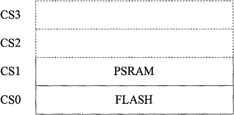
[0063] Use the address space not occupied by FLASH and PSRAM in CS0 and CS1 to enable LCD and DSP external devices, but the external devices that can be enabled are not limited to the above four devices, and correspond to other external devices in other systems device, the chip select signal extension method is also applicable.

[0064] The FLASH and PSRAM in CS0 and CS1 cannot occupy all the space allocated by the system in some systems, and the remaining space can be used and allocated to other external devices. This method can effectively save space and reduce costs.

[0065] In this specific embodiment, the internal operation logic of the chip is as follows: Figure 4 and Figure 5 As shown, preferably EA24 is the chip select input reference signal, but it is not limited to EA24. In different systems, any address bit in the 32-bit address that will not affect other devices can be selected as the chip select input reference signal. In this embodiment, according to the phot...

specific Embodiment 2

[0076] Use the address space not occupied by PSRAM in CS1 to enable LCD and DSP external devices, and CS0 is still exclusively occupied by FLASH. The external devices that can be enabled are not limited to the above four devices, and the chip selection signal extension method is also applicable to other external devices in other systems.

[0077] Considering that FLASH needs to occupy a relatively large space in some cases, CS0 can only meet the space requirements of FLASH, while PSRAM in CS1 occupies a small space in some systems and cannot occupy all the space allocated by the system. The space is utilized and allocated to other external devices. This method can effectively save space and reduce costs.

[0078] In this specific embodiment, the internal operation logic of the chip is as follows: Figure 7 As shown, preferably EA23 and EA24 are chip select input reference signals, but not limited to EA23 and EA24, in different systems, any two address bits in the 32-bit addr...

specific Embodiment 3

[0088] Use CS2, CS3 unencapsulated free address space to enable LCD and DSP external devices, CS0, CS1 are still exclusively occupied by FLASH and PSRAM, but the external devices that can be enabled are not limited to the above four devices, Corresponding to other external devices in other systems, the chip selection signal extension method is also applicable.

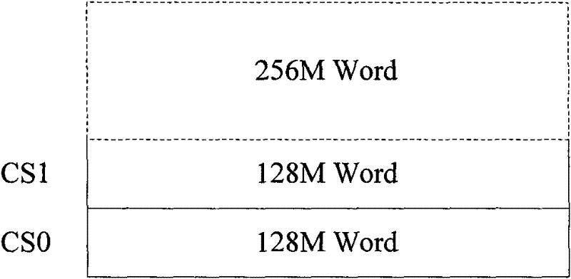
[0089] In some systems, FLASH and PSRAM occupy a large space, and the remaining space cannot meet the needs of other devices. In the baseband chip, although only two address spaces, CS0 and CS1, are divided, there is still 512M free space. Address space that can be allocated to other external devices. If the 512M space is divided into two new address spaces, CS2 and CS3, such as Figure 9 As shown, like CS0 and CS1, it can also serve new external devices. This method can add a new external device interface without affecting the original address space division of the baseband chip, effectively saving space and reducin...


PUM


Abstract

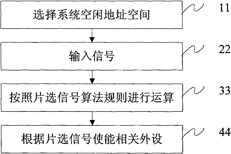
The invention discloses a chip select signal spreading method, which comprises the following steps: selecting a free address space of a system; inputting a signal; performing operation according to a chip select signal spreading algorithm rule; and enabling related peripheral equipment according to the chip select signal. On the basis of not changing a hardcore of the system, the free address space can be used, chip select signals of new hardware are spread besides previous chip select signals of the system, and the peripheral equipment connected with the system previously cannot be influenced. By using the free address space, existing resources can be effectively utilized, and additional cost is not required to be increased. The chip select signal spreading method has strong practicability, hardly increases additional load for the system, can be applied to the field of control signal generation and transmission and is suitable for various baseband chips.

Description

technical field [0001] The invention relates to a control signal generation and transmission technology, in particular to a chip selection signal expansion method. Background technique [0002] In current electronic products, more and more designers and users hope to add more functions to the products while controlling the cost. This requires expanding the hardware interface without enhancing the main control chip of the system. Taking the MTK6223D baseband chip as an example, the system includes 1G space, and divides two address spaces CS0 and CS1 for chip select signals. But when only CS0 and CS1 are used, not only the remaining address space is wasted, but also only two external devices can be enabled for these two address spaces. The system cannot be completed when more external devices need to be connected, and interfaces need to be added to the hardware structure of the product. Other baseband chips have similar problems. [0003] There are at least the following d...

Claims


Application Information

Patent Timeline
Patent Type & Authority Patents(China)
IPC IPC(8): G06F13/40
Inventor 程杰唐冕刘志碧陈杰
Owner BEIJING SUPERPIX MICRO TECHNOLOGY CO LTD
Learn More