

High-density low-parasitic capacitor
A capacitor device, low parasitic technology, applied in circuits, electrical components, electro-solid devices, etc., can solve problems such as restricting applications and affecting circuit performance, reducing additional power consumption, improving performance, and achieving significant effects
- Summary
- Abstract
- Description
- Claims
- Application Information
AI Technical Summary
Problems solved by technology
Method used
Image

Examples
Embodiment Construction
[0027] In order to make the objectives, technical solutions, and advantages of the present invention clearer, the following further describes the present invention in detail with reference to specific embodiments and drawings.
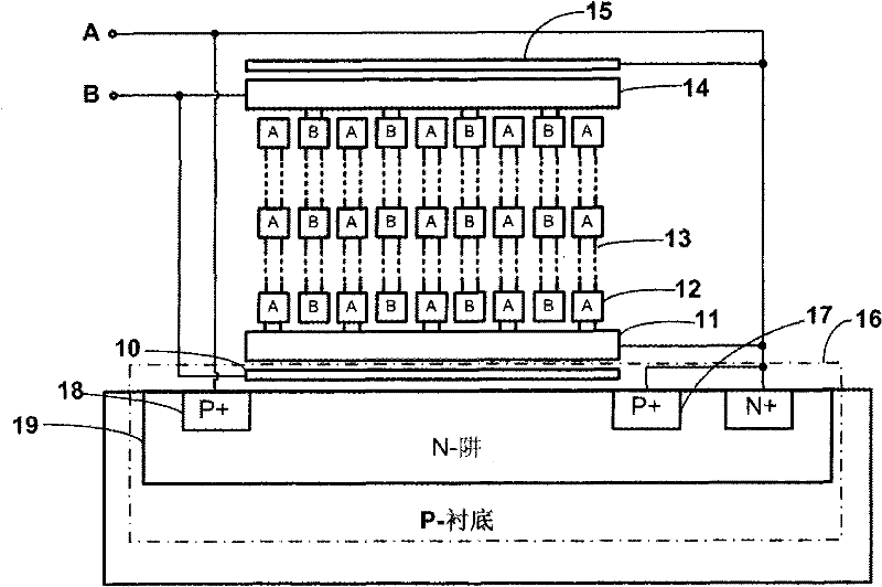
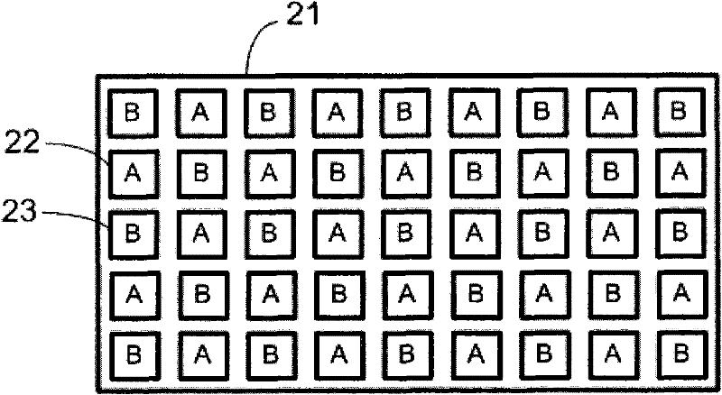
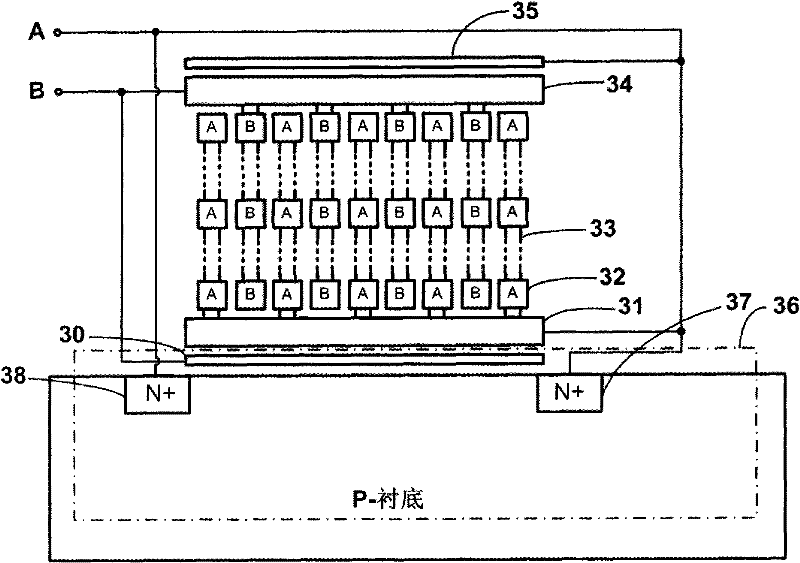
[0028] The high-density and low-parasitic capacitor device proposed by the present invention firstly maximizes the capacitance per unit area, and secondly can effectively reduce the parasitic capacitance from the N well to the P substrate in the PMOS capacitor. In addition, the present invention uses The special interlayer metal interconnection structure can maximize the capacitance between the same metal layer and the capacitance between the through hole and the through hole. As the feature size of the process decreases, the lithography accuracy increases, and the number of metal layers increases, The distance between the metal layer and the metal layer, and the distance between the through hole and the through hole can be further reduced, and the effecti...
PUM
 Abstract
Description
Claims
Application Information