GMSK (Guassian Minimum Shift Keying) modulation device and method
A technology for modulating signals and data, applied in the field of GMSK modulation devices, can solve the problems of large chip area and large ROM space occupation, and achieve the effect of small chip area and reduced ROM occupation
- Summary
- Abstract
- Description
- Claims
- Application Information
AI Technical Summary
Problems solved by technology
Method used
Image
Examples
Embodiment Construction
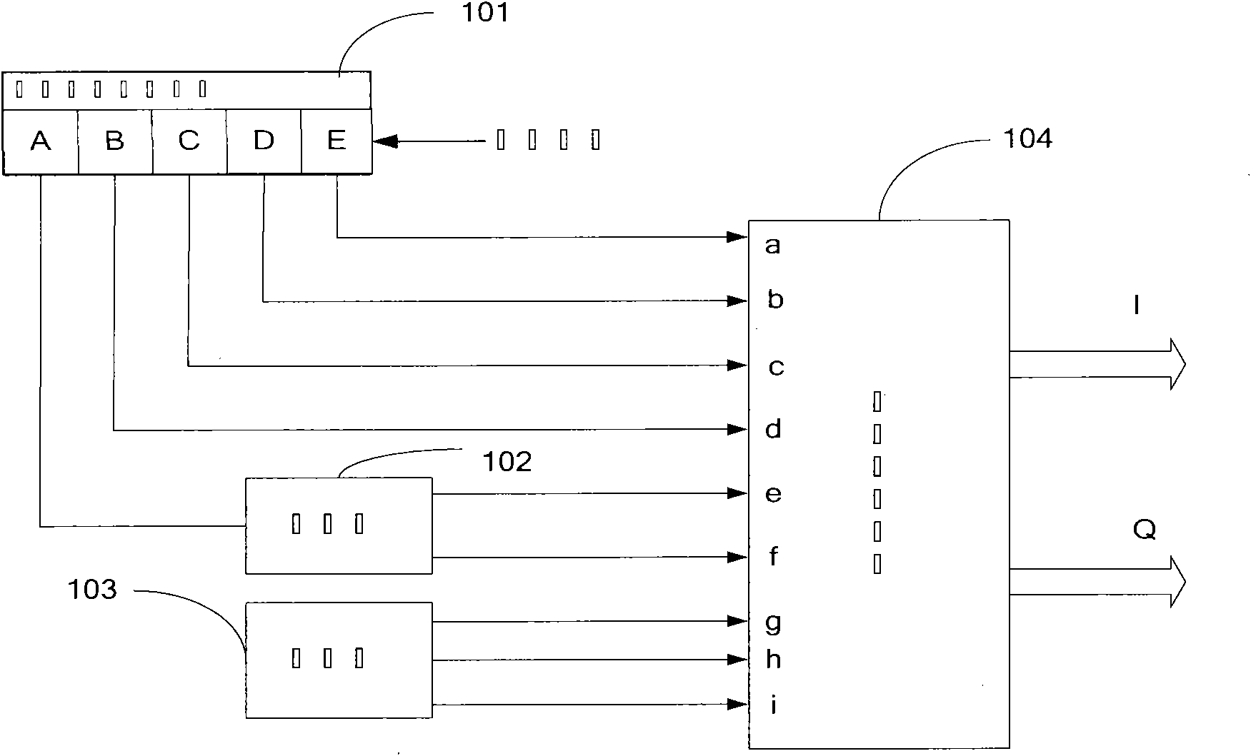
[0077] figure 1 Shown is a schematic structural diagram of a GMSK modulation device implemented by using a look-up table method in the prior art. The working process of the GMSK modulation device includes: after the input signal is shifted by the first data processing module 101, the obtained highest bit (the position shown by A in the figure) data is sent to the accumulator 102 for accumulation operation, and The accumulative result is sent into the address interfaces shown in e and f of the data reading module 104 respectively in high and low order, wherein position e shown in the figure is a high address interface; Arrangement to high order (i.e. the order shown in E, D, C, B in the figure), and send it into the high four-bit address interface arranged from high to low in the data reading module 104 (i.e. a, b, c in the figure , d arrangement sequence shown in the position). The three output signals generated by the counter 103 are sent into the low three-bit address inte...
PUM
 Abstract
Description
Claims
Application Information


