Method of manufacturing optical receiver module and apparatus for manufacturing the same

An optical receiver and optical connector technology, which is applied in the coupling of optics, optical components, optical waveguides, etc., can solve problems such as difficult core adjustment, and achieve the effect of achieving desired characteristics

Inactive Publication Date: 2010-12-01
RENESAS ELECTRONICS CORP
View PDF7 Cites 3 Cited by
  • Summary
  • Abstract
  • Description
  • Claims
  • Application Information

AI Technical Summary

Problems solved by technology

[0011] Due to the above circumstances, in the manufacture of optical receiver modules including planar PIN-PDs, it is difficult to perform core adjustment in a short time

Method used


Image

  • Method of manufacturing optical receiver module and apparatus for manufacturing the same
  • Method of manufacturing optical receiver module and apparatus for manufacturing the same
  • Method of manufacturing optical receiver module and apparatus for manufacturing the same

Examples


no. 1 example

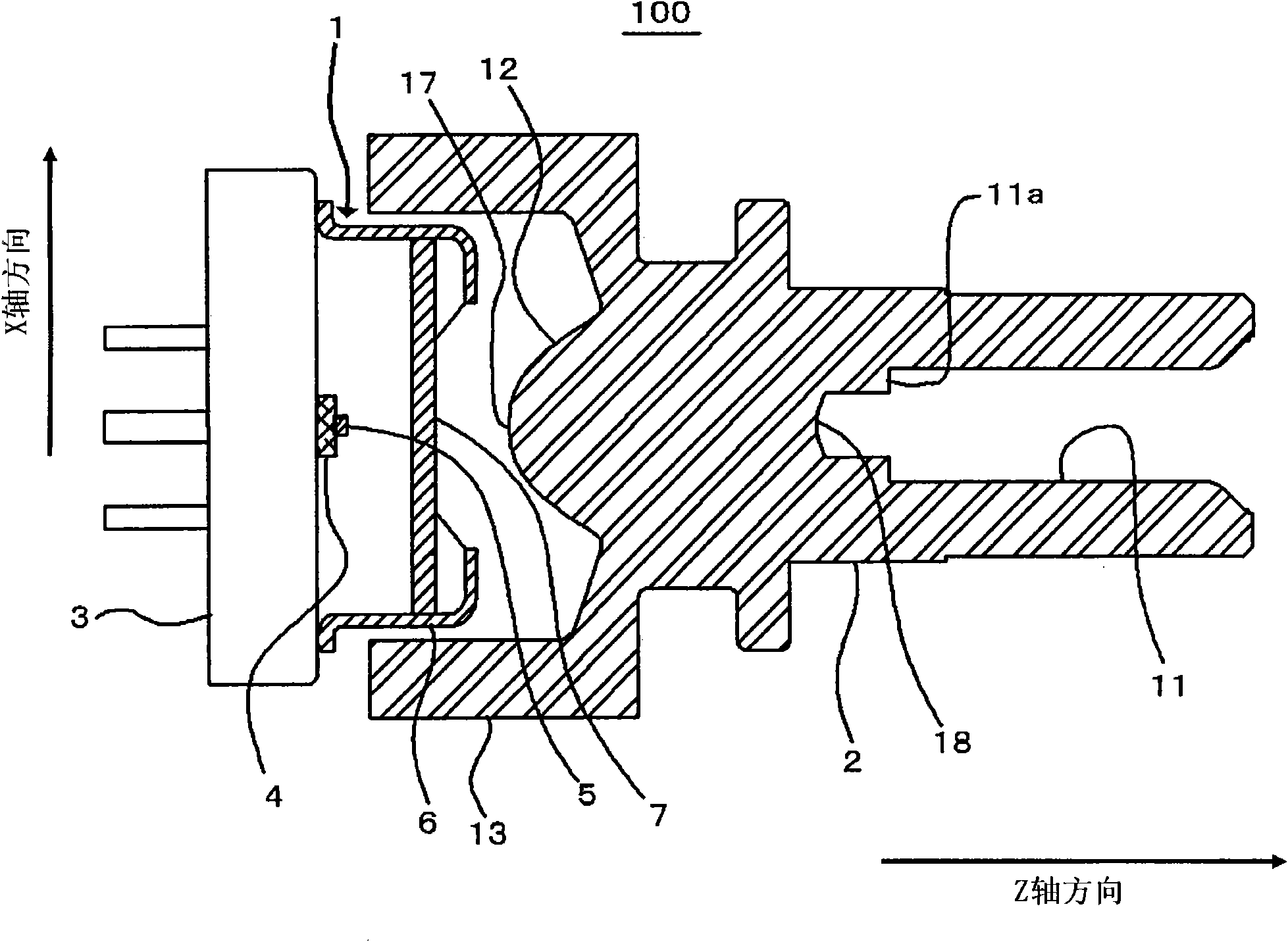
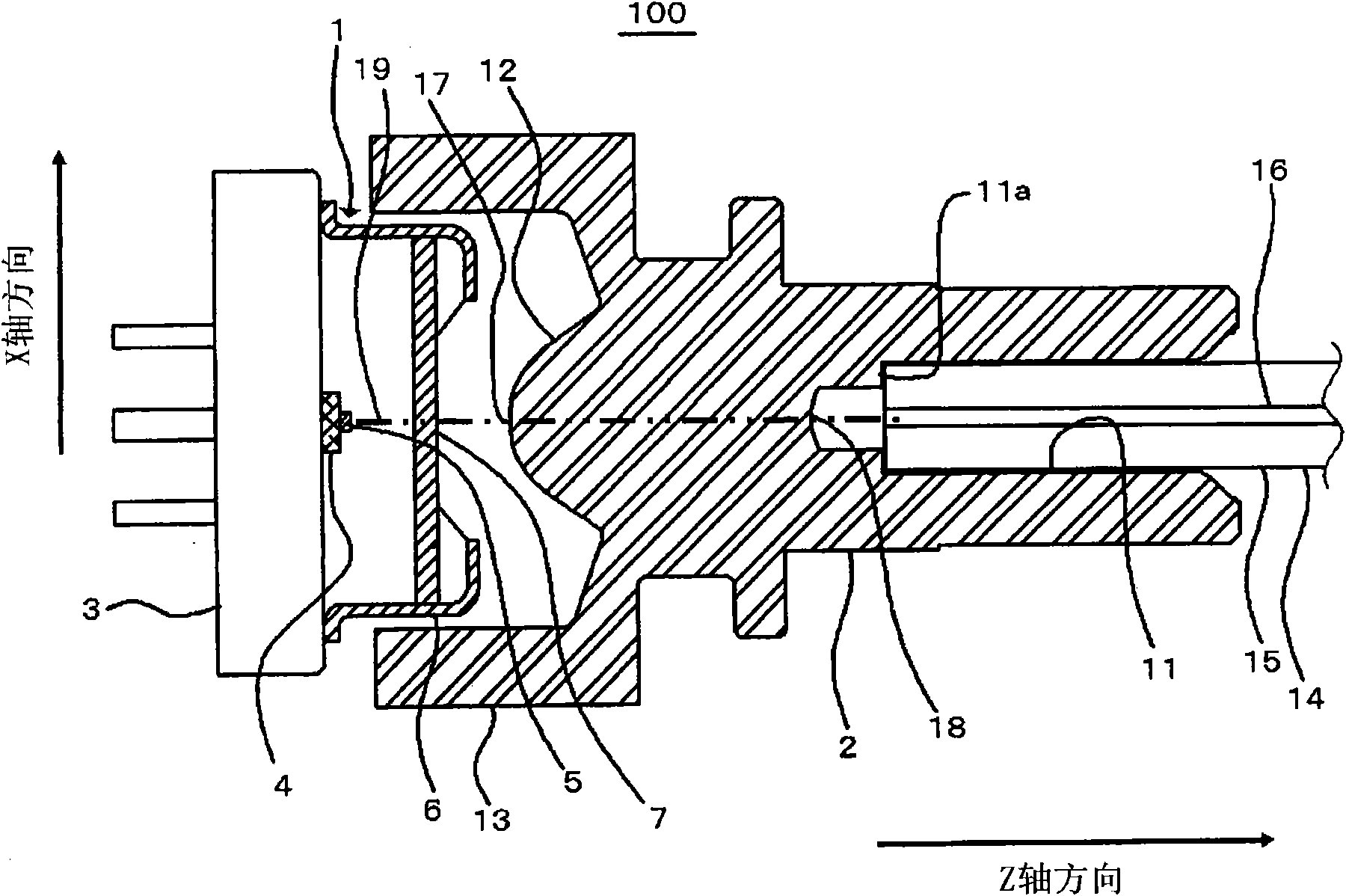
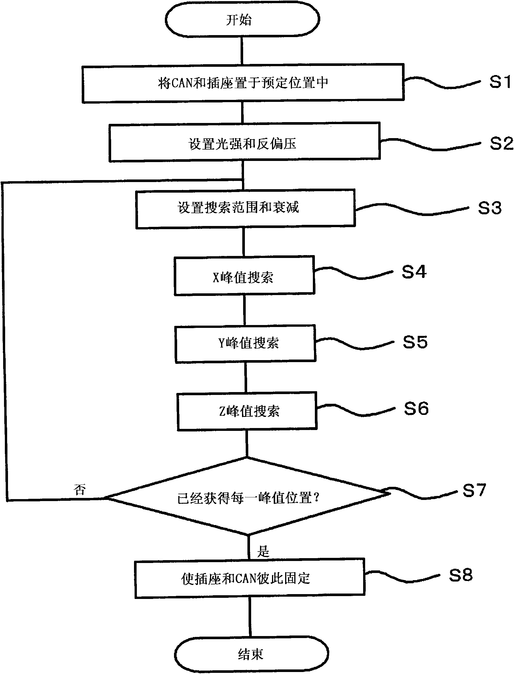
[0067] figure 1 is a cross-sectional view showing the structure of the optical receiver module 100 manufactured by the method for manufacturing the optical receiver module according to the first embodiment. figure 2 is to indicate that the optical connector 14 is inserted into the figure 1 A cross-sectional view of the situation of the optical receiver module 100. image 3 is a flowchart representing a method for manufacturing an optical receiver module according to the first embodiment. Figure 4 Indicates the light intensity distribution on the end face of the optical fiber connected to receptacle 2. Figure 5 Indicates the photocurrent varying with the position of the socket 2 in the X-axis direction. Figure 6 Indicates the photocurrent depending on the position of the socket 2 in the Z-axis direction. Figure 7 is a block diagram showing the structure of the optical receiver module manufacturing apparatus 150 according to the first embodiment.

[0068] The optical ...

no. 2 example

[0180] In the first embodiment described above, the method for manufacturing an optical receiver module is applied to the optical receiver module 100 having the lens 12 embedded in the socket 2 . On the other hand, in the second embodiment, the method for manufacturing an optical receiver module is applied to a Figure 12 The structure of the optical receiver module 200 is shown.

[0181] Such as Figure 12 As shown, an optical receiver module 200 to which the method for manufacturing an optical receiver module according to the present embodiment is applied includes a CAN 1 and a socket 2 (without a built-in lens).

[0182] The CAN 1 includes the same stem 3, the same carrier 4, and the same light-receiving element 5 as those of the first embodiment. In this embodiment, a transimpedance amplifier, a capacitor, etc., as well as a carrier 4 and a light receiving element 5 can be mounted on the stem 3 .

[0183] In this embodiment, the CAN 1 has a cap 21 instead of the cap 6 o...


PUM


Abstract

The core adjusting process includes a procedure of searching for the position in which the photocurrent of the light-receiving element reaches its peak in each of the X-, Y-, and Z-directions. In the searching procedure, the light emitted from a multimode fiber of a MCP is gathered by a lens and is transmitted to the light-receiving element. A check is then made to determine whether, at in both directions of the search direction, there exist a first and second attenuation positions in which the photocurrent shows a predetermined attenuation relative to a peak value in a search range. If there exist the attenuation positions, a peak position is determined to be a position located within a second predetermined range from the middle point between the attenuation positions, and the relative positions of the receptacle and the CAN package are adjusted to the peak position.

Description

[0001] Cross References to Related Applications [0002] This application is based on Japanese Patent Application No. 2009-130090, the entire contents of which are incorporated herein by reference. technical field [0003] The invention relates to a method of manufacturing an optical receiver module and a device for manufacturing an optical receiver module. Background technique [0004] First, a general structure of a semiconductor optical receiver module (optical receiver module) including a planar light receiving element (photodiode (PD)) is described. [0005] An optical receiver module including a planar light receiving element includes a stem, a carrier on the stem, and a planar light receiving element on the carrier. Carriers and light receiving elements, transimpedance amplifiers (TIA), capacitors for noise reduction, etc. can also be mounted on the header. The optical receiver module further includes a cap (such as a flat window cap with a flat window) that hermeti...

Claims


Application Information

Patent Timeline
Patent Type & Authority Applications(China)
IPC IPC(8): G02B6/42
CPCG02B6/3809G02B6/4206G02B6/4292G02B6/4225
Inventor 栗原佑介森林茂
Owner RENESAS ELECTRONICS CORP
Why Eureka
Try Eureka