

Lithographic method and arrangement
A technology of lithography and pattern features, applied in microlithography exposure equipment, photolithography exposure equipment, optics, etc., can solve problems such as difficult to achieve
- Summary
- Abstract
- Description
- Claims
- Application Information
AI Technical Summary
Problems solved by technology
Method used
Image


Examples
Embodiment Construction
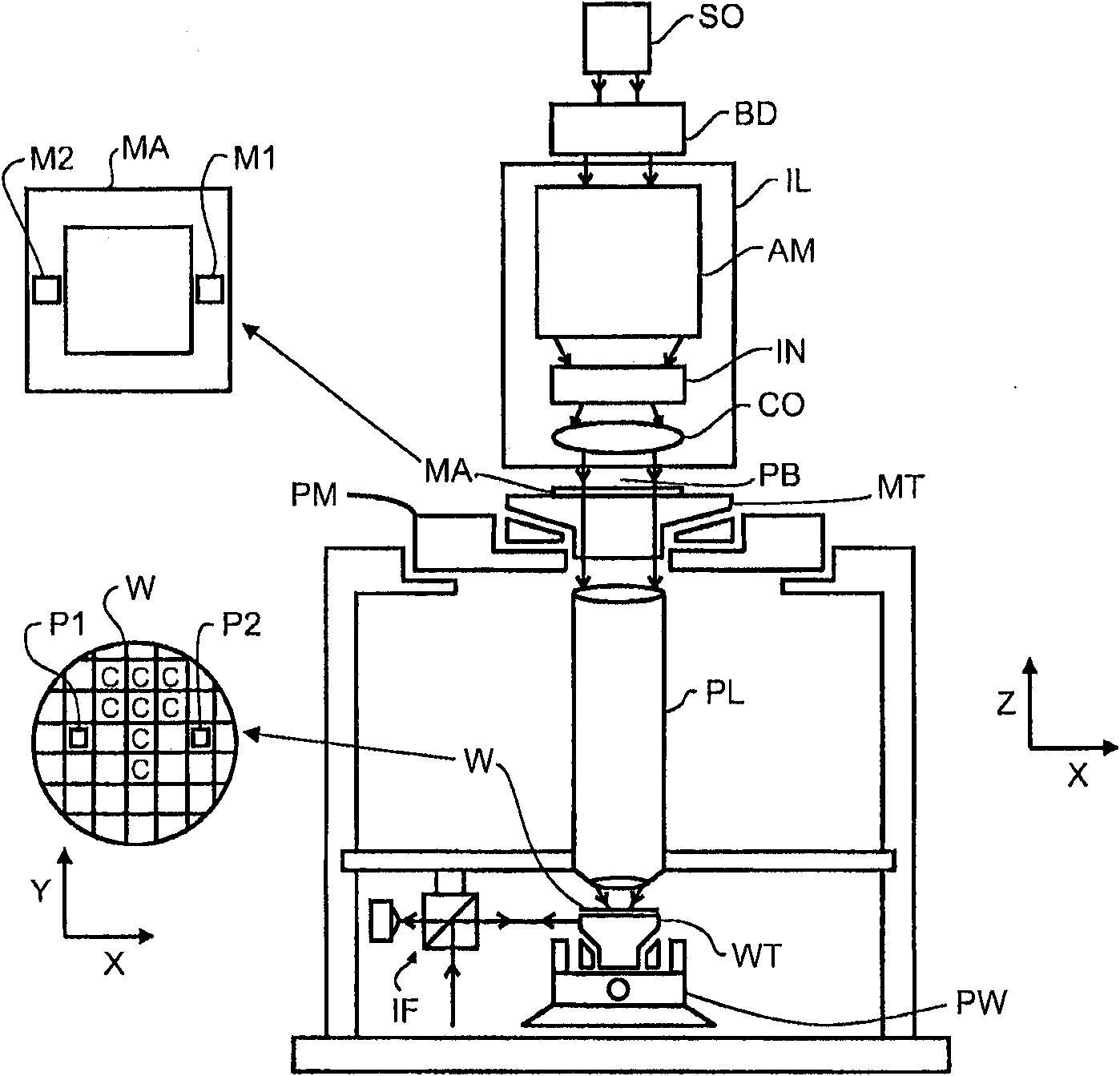
[0030] Although specific reference is made herein to lithographic apparatus for IC fabrication, it should be understood that the lithographic apparatus described herein may have other applications for fabricating components with microscale, and even nanoscale features, such as for fabricating integrated optical systems, magnetic Guidance and detection patterns for domain memories, liquid crystal displays (LCDs), thin-film magnetic heads, etc. Those skilled in the art will appreciate that, in the case of this alternate application, any term "wafer" or "die" used therein may be considered synonymous with the more general term "substrate" or "target portion", respectively. righteous. The substrate referred to here can be processed before or after exposure, such as in a track (a tool that typically applies a layer of resist to a substrate and develops the exposed resist), a metrology tool and / or in the inspection tool. Where applicable, the disclosure herein may be employed in s...
PUM
 Abstract
Description
Claims
Application Information