Double sided organic light emitting diode (OLED)

A double-sided light-emitting, diode technology, applied in the direction of diodes, electroluminescent light sources, light sources, etc.

Inactive Publication Date: 2011-01-19
KONINKLIJKE PHILIPS ELECTRONICS NV
View PDF2 Cites 18 Cited by
  • Summary
  • Abstract
  • Description
  • Claims
  • Application Information

AI Technical Summary

Problems solved by technology

Unfortunately, each single layer is transparent
Thus, the OLED is only suitable for emitting either the color of the first emitting layer or the color of the second emitting layer, or a mixed color emitting

Method used


Image

  • Double sided organic light emitting diode (OLED)
  • Double sided organic light emitting diode (OLED)

Examples


Embodiment Construction

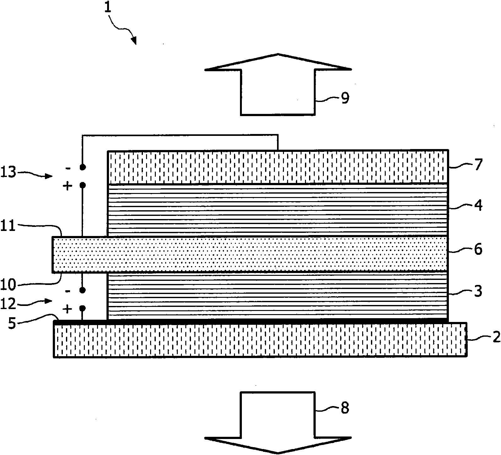
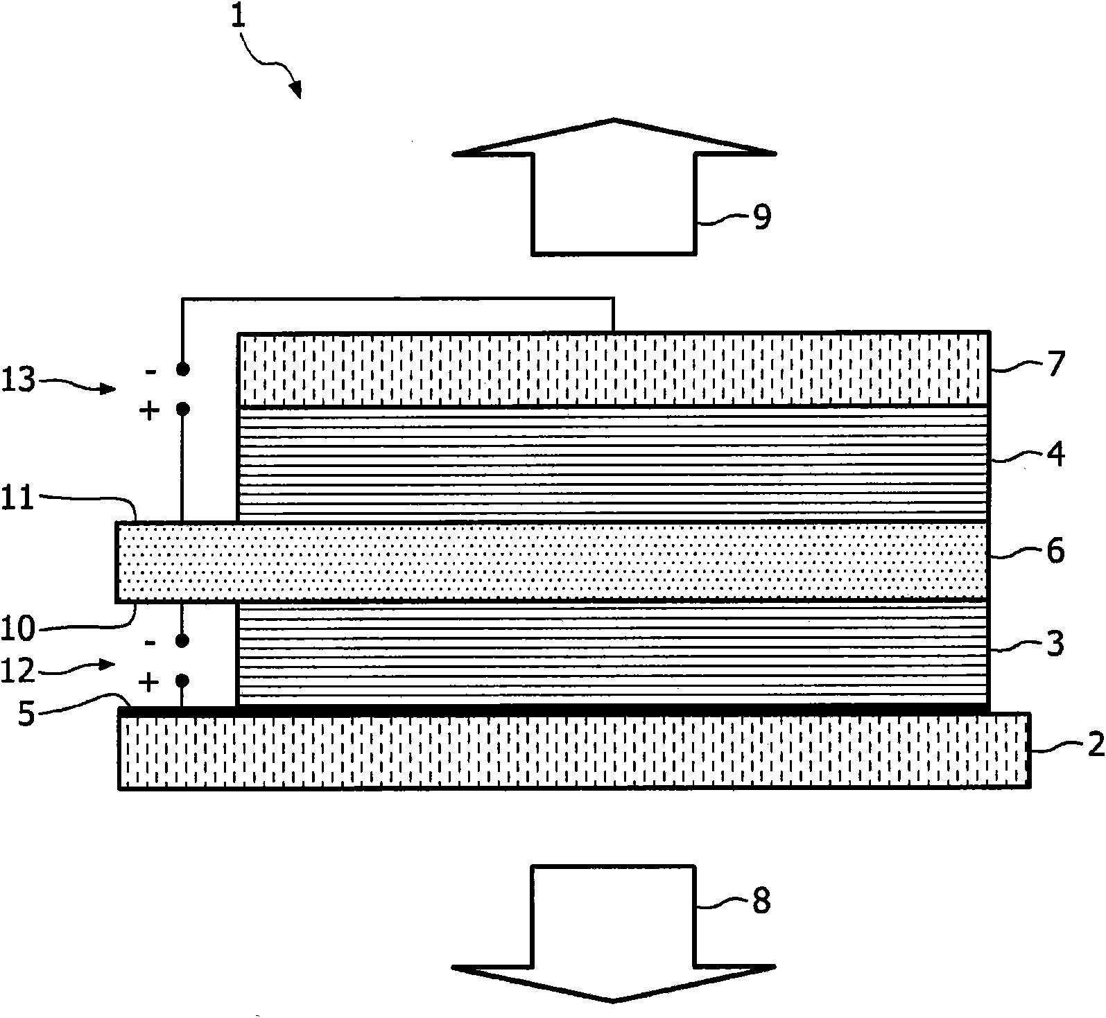
[0021] figure 1The embodiment described in comprises a layer sequence to provide a double-sided light-emitting diode device 1 . The substrate layer 2 is realized as a carrier, on which the layer series is deposited on only one side. The series of layers comprises at least: a bottom electrode layer 5; followed by a first organic stack, i.e. one or more layers of organic material, comprising a first emissive layer 3; followed by a non-transparent charge generation layer 6; followed by a second An organic stack, ie one or more layers of organic material, comprising a second emissive layer 4 ; where the last layer is realized by a transparent top electrode layer 7 . This layer series is characterized by only a basic structure. Additional layers can be deposited between said layers to increase efficiency, or to increase durability by applying a protective layer like a glass cover or a thin film layer acting as a cover layer. The power supply for the first emitting layer 3 and th...


PUM


Abstract

The invention relates to a double sided light emitting diode device (1) comprising a transparent substrate layer (2) with a layer system, featuring at least a first emitting layer (3) and at least a second emitting layer (4).

Description

technical field [0001] The invention relates to a double-sided light-emitting diode device comprising a transparent substrate layer having a layer system characterized by comprising at least a first emitting layer and at least a second emitting layer. Background technique [0002] Double-sided light-emitting diode devices are known from the prior art as light-emitting devices which are adapted to emit light in two different directions. When different emissive layers are stacked on top of each other, each layer may operate separately or a number of individual layers may operate in a common manner. Thus, different colors can be emitted through the substrate layer and can be emitted through the top side of the device in the top side direction. Typically the substrate layer forms the bottom of the device, otherwise known as an OLED. These organic light-emitting diode-based bottom-emitting or top-emitting lighting devices have received a lot of attention as excellent flat panel...

Claims


Application Information

Patent Timeline
Patent Type & Authority Applications(China)
IPC IPC(8): H01L27/32F21K7/00H05B33/14F21K99/00
CPCH01L27/3209H01L51/5278H01L27/3267H10K59/32H10K59/128H10K50/19H05B33/02H10K50/814H10K50/824H10K50/85H10K50/30
Inventor S·P·格拉博夫斯基C·M·戈尔德曼
Owner KONINKLIJKE PHILIPS ELECTRONICS NV
Why Eureka
Try Eureka