Method for making gate oxide layer and gate polysilicon layer

A technology of polysilicon layer and gate oxide layer, which is applied in semiconductor/solid-state device manufacturing, electrical components, circuits, etc.

Inactive Publication Date: 2012-02-08
SEMICON MFG INT (SHANGHAI) CORP
View PDF3 Cites 0 Cited by
  • Summary
  • Abstract
  • Description
  • Claims
  • Application Information

AI Technical Summary

Problems solved by technology

The gate oxide layer is very easy to oxidize in the air, and a gate oxide layer thickness of about 0.5 to 1 angstrom can be grown in 0.5 hours, and the thickness of the gate oxide layer is inherently very thin, and a slight change in the thickness will lead to degradation of device performance. reduce

Method used


Image

  • Method for making gate oxide layer and gate polysilicon layer
  • Method for making gate oxide layer and gate polysilicon layer
  • Method for making gate oxide layer and gate polysilicon layer

Examples


Embodiment Construction

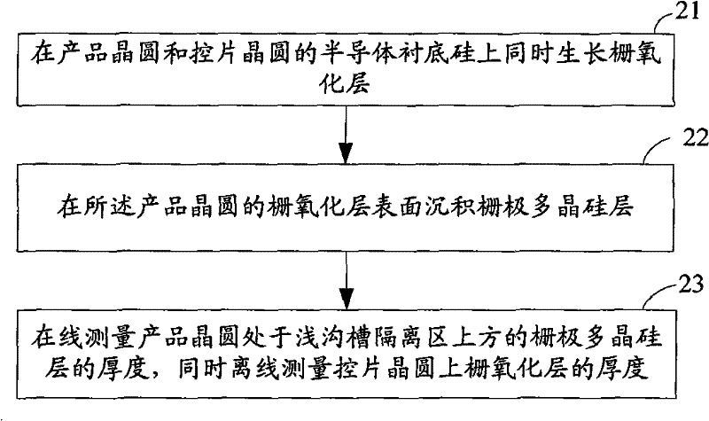
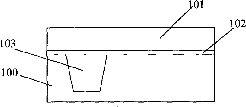
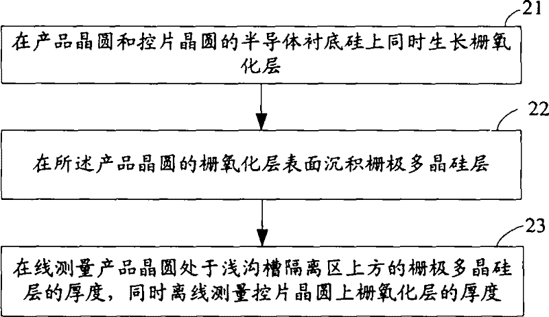
[0026] Step 21, growing a gate oxide layer on the semiconductor substrate silicon. These include simultaneous growth of a gate oxide layer on the semiconductor substrate silicon of the product wafer and the control wafer. Among them, the control wafer is a flat silicon wafer that has not been processed by a process, and is used during testing. When the thickness of the gate oxide layer needs to be measured, the control wafer is placed into the reaction chamber, and after the growth of the gate oxide layer is completed, only the control wafer with the gate oxide layer grown is output from the reaction chamber for thickness measurement;

[0027] Step 22, depositing a gate polysilicon layer on the surface of the gate oxide layer. Because only the thickness of the gate oxide layer on the control wafer needs to be measured offline, there is no need to deposit the gate polysilicon layer on the control wafer at this time, that is to say, only deposit the gate polysilicon layer on th...


PUM


Abstract

The invention discloses a method for manufacturing a gate oxide layer and a gate polysilicon layer, comprising: simultaneously growing a gate oxide layer on the semiconductor substrate silicon of a product wafer and a control wafer; The gate polysilicon layer is deposited on the surface of the layer; the thickness of the product wafer gate polysilicon layer is measured online, and the thickness of the gate oxide layer on the control wafer is measured offline. Using this method can prevent the gate oxide layer from being oxidized when it is exposed to air during the measurement process.

Description

technical field [0001] The invention relates to a semiconductor device manufacturing process, in particular to a method for making a gate oxide layer and a gate polysilicon layer. Background technique [0002] At present, with the development of semiconductor technology, the operating speed of semiconductor devices is getting faster and faster, the integration of chip circuits is getting higher and higher, and the power consumption is getting lower and lower, so that the characteristic size of the gate polysilicon layer of semiconductor devices Parameters such as the thickness of the gate oxide layer (Gate Oxide) gradually become smaller. A semiconductor device includes a core (core) area and an peripheral circuit (IO) area. Among them, the growth thickness of the gate oxide layer in the core area is relatively thin, about less than 20 angstroms; the peripheral area of ​​the core area is called the peripheral circuit area, which is about 50-100 angstroms. Thickness measure...

Claims


Application Information

Patent Timeline
Patent Type & Authority Patents(China)
IPC IPC(8): H01L21/283H01L21/66
Inventor 唐兆云何有丰
Owner SEMICON MFG INT (SHANGHAI) CORP
Why Eureka
Try Eureka