Annealing apparatus

An annealing device and light-emitting element technology, which is applied in the manufacture of electrical components, semiconductor/solid-state devices, circuits, etc., can solve the problems of large LED loss, reduced LED luminous amount, and reduced efficiency, so as to reduce losses and suppress the reduction of luminous amount Effect

Inactive Publication Date: 2011-03-02
TOKYO ELECTRON LTD
View PDF0 Cites 6 Cited by
  • Summary
  • Abstract
  • Description
  • Claims
  • Application Information

AI Technical Summary

Problems solved by technology

Therefore, when driving high-brightness LEDs, use the existing PWM control to drive the LEDs (PWM drive), although the loss of the control part can be reduced, but the loss of the LED part increases in proportion to the control current. When the brightness (light quantity) of the control is controlled, the loss of the LED is relatively large
In addition, the reduction in efficiency and the reduction in the amount of light emitted by the LED due to heat due to this loss will become problems.

Method used


Image

  • Annealing apparatus
  • Annealing apparatus
  • Annealing apparatus

Examples


Embodiment Construction

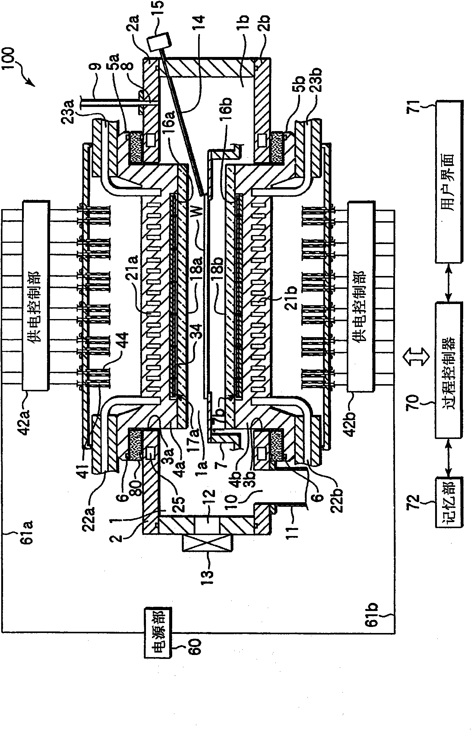
[0025] Hereinafter, embodiments of the present invention will be described with reference to the drawings. Here, an annealing apparatus for annealing a wafer with impurities implanted on its surface will be described as an example.

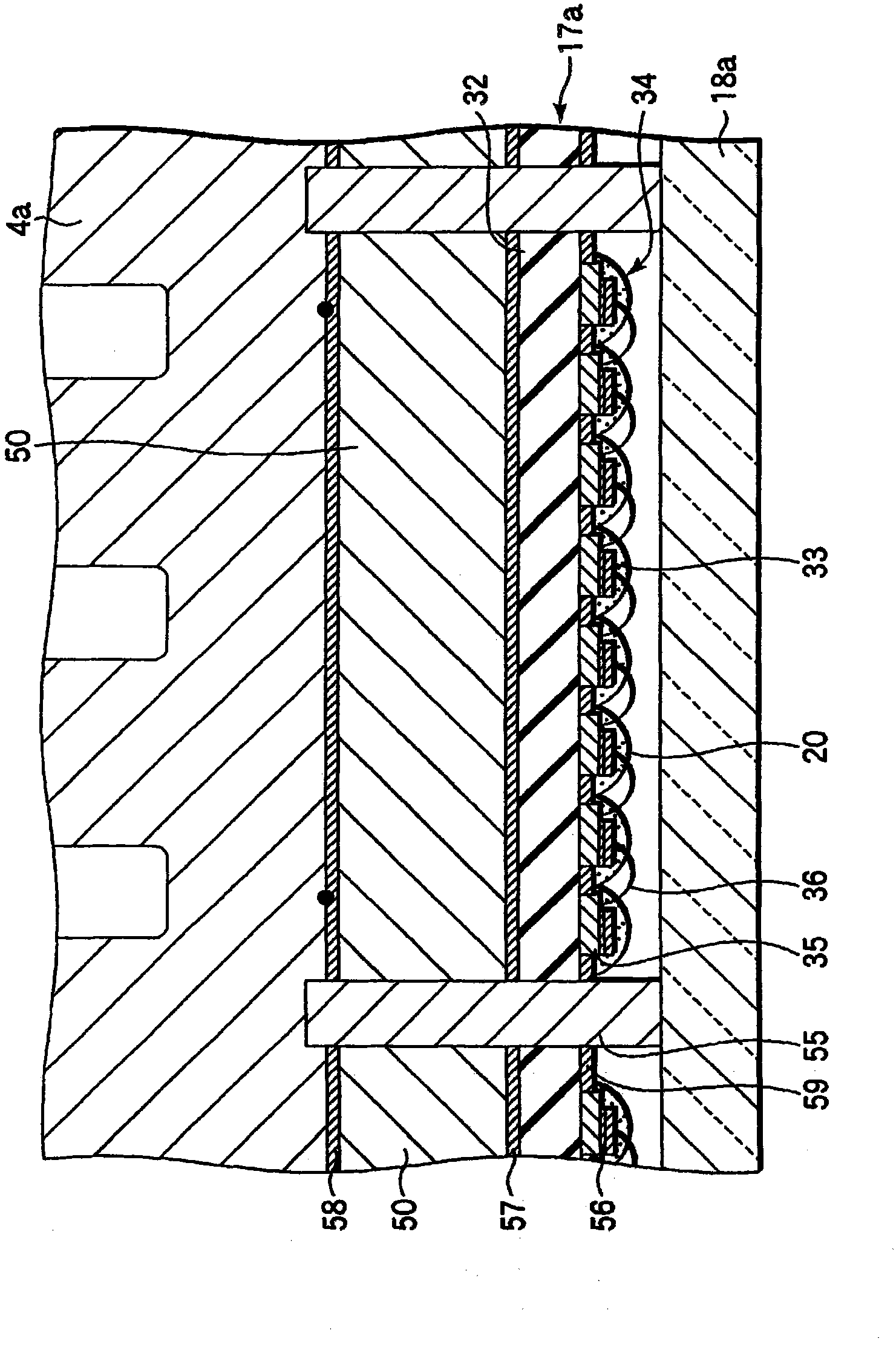
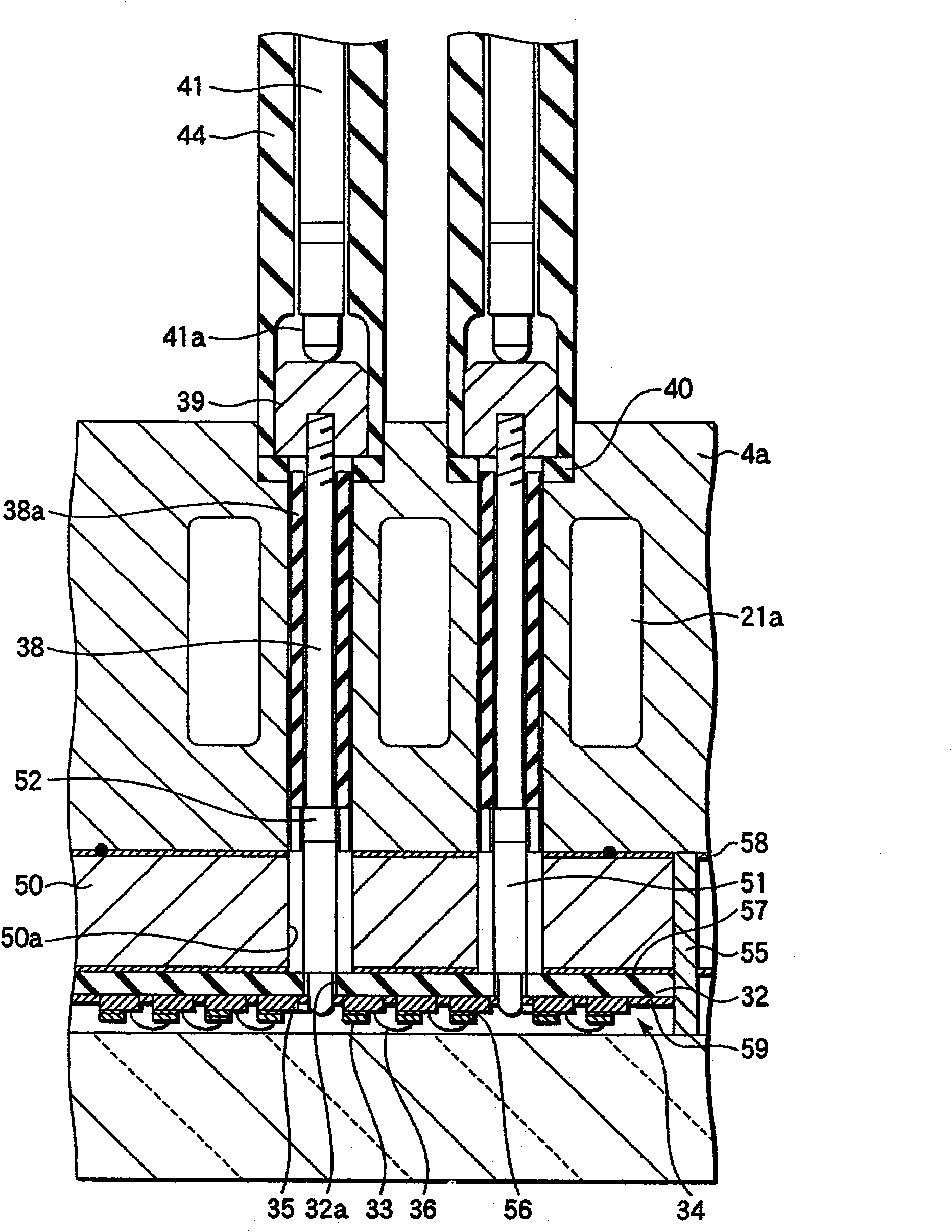
[0026] figure 1 It is a cross-sectional view showing a schematic configuration of an annealing apparatus according to an embodiment of the present invention. figure 2 yes means figure 1 An enlarged cross-sectional view of the heating source of the annealing apparatus. image 3 yes means figure 1 An enlarged cross-sectional view of the power supply portion of the LED of the annealing device.

[0027] This annealing apparatus 100 is constituted by a seal, and has a processing chamber 1 into which a wafer W is loaded. The processing chamber 1 has a columnar annealing section 1a in which a wafer W is arranged, and an annular gas diffusion section 1b provided outside the annealing section 1a. The height of the gas diffusion part 1b is higher tha...


PUM


Abstract

An annealing apparatus is provided with a chamber (2) wherein a wafer (W) is stored; heating sources (17a, 17b) having a plurality of LEDs (33) for irradiating the wafer (W) in the chamber (2) with light; a power supply section (60) for feeding the LEDs (33) of the heating sources (17a, 17b) with power; power feed control sections (42a, 42b) which control power feed from the power supply section (60) to a light emitting element; light transmitting members (18a, 18b) which transmit light emitted from the LEDs (33); and an air-releasing mechanism for releasing air from inside the chamber (2). The power feed control sections (42a, 42b) drive the LEDs (33) with direct current.

Description

technical field [0001] The present invention relates to an annealing apparatus for performing annealing by irradiating a semiconductor wafer or the like with light from a light emitting element such as a light emitting diode (LED). Background technique [0002] In the manufacture of semiconductor devices, although there are various heat treatments such as film formation treatment, oxidation diffusion treatment, modification treatment, annealing treatment, etc. on semiconductor wafers (hereinafter simply referred to as wafers) as substrates to be processed, with the development of semiconductor devices Higher speed and higher integration are required, especially in the annealing after ion implantation, in order to minimize diffusion, there is a need for higher speed temperature rise and fall. As an annealing apparatus capable of raising and lowering the temperature at such a high speed, it has been proposed to use a light emitting diode (LED) as a light emitting element as a ...

Claims


Application Information

Patent Timeline
IPC IPC(8): H01L21/26H01L21/31
CPCH01L21/67115H01L21/67098H01L21/324H01L21/2686
Inventor 河西繁铃木智博
Owner TOKYO ELECTRON LTD
Why Eureka
Try Eureka