Lead frame for carrying out ceramic double in-line package (CDIP) on chips

A dual-in-line package and lead frame technology, which is applied in the direction of electrical components, electric solid devices, circuits, etc., can solve the problems of prolonging the packaging cycle, increasing the production cost, and bonding contact pads, etc., so as to prolong the packaging cycle and increase the High production cost and the effect of saving the number of pins

Inactive Publication Date: 2011-03-30
SEMICON MFG INT (SHANGHAI) CORP
View PDF0 Cites 1 Cited by
  • Summary
  • Abstract
  • Description
  • Claims
  • Application Information

AI Technical Summary

Problems solved by technology

[0006] In view of this, the present invention provides a lead frame for ceramic dual-in-line packaging of chips, which can solve the problem that all contact pads of the chip cannot be wired due to insufficient pins on the lead frame 102, and does not require It will increase the production cost and lengthen the packaging cycle

Method used


Image

  • Lead frame for carrying out ceramic double in-line package (CDIP) on chips
  • Lead frame for carrying out ceramic double in-line package (CDIP) on chips
  • Lead frame for carrying out ceramic double in-line package (CDIP) on chips

Examples


Embodiment Construction

[0022] In order to make the objectives, technical solutions and advantages of the present invention clearer, the present invention will be further described in detail below with reference to the accompanying drawings and embodiments.

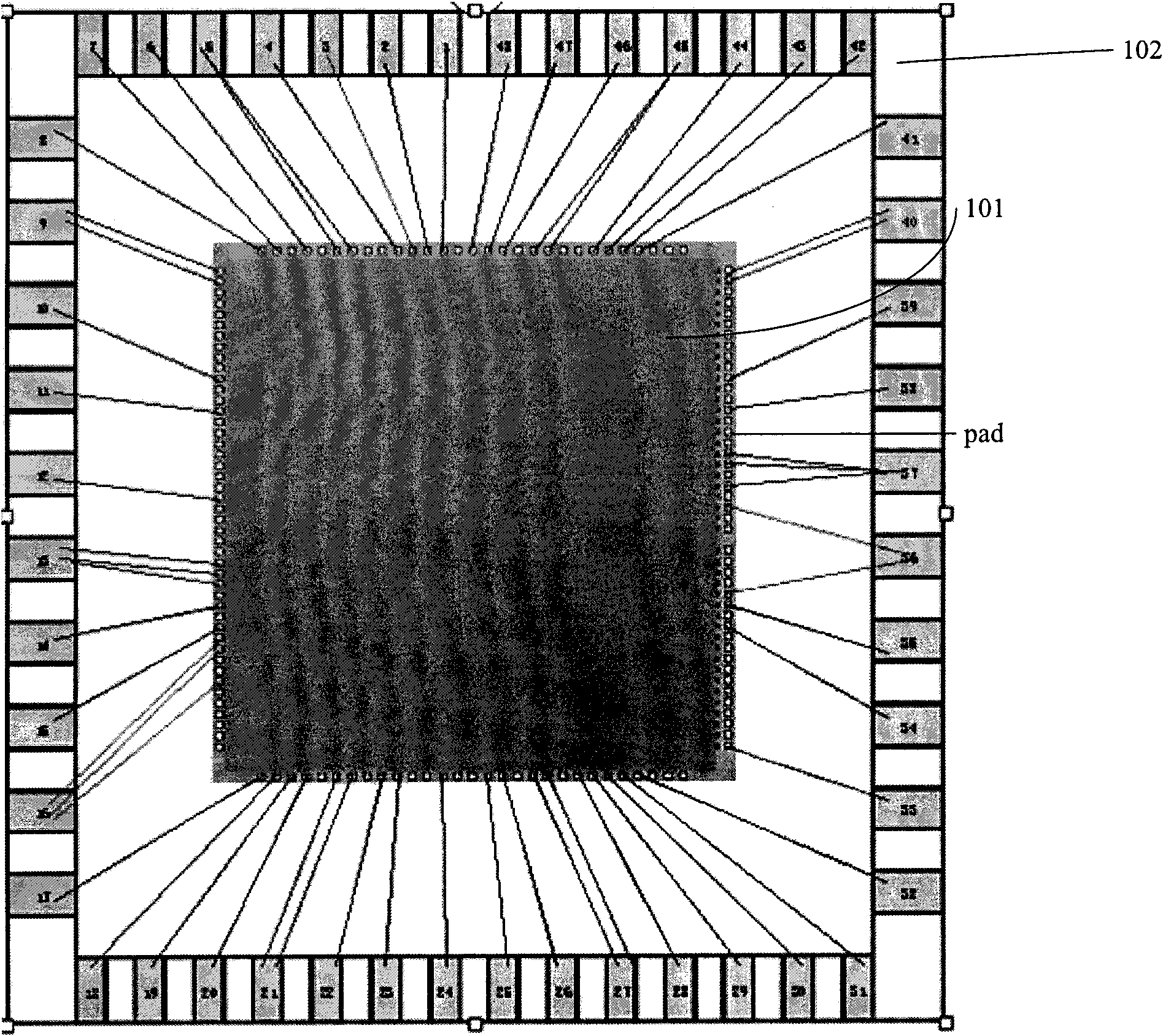
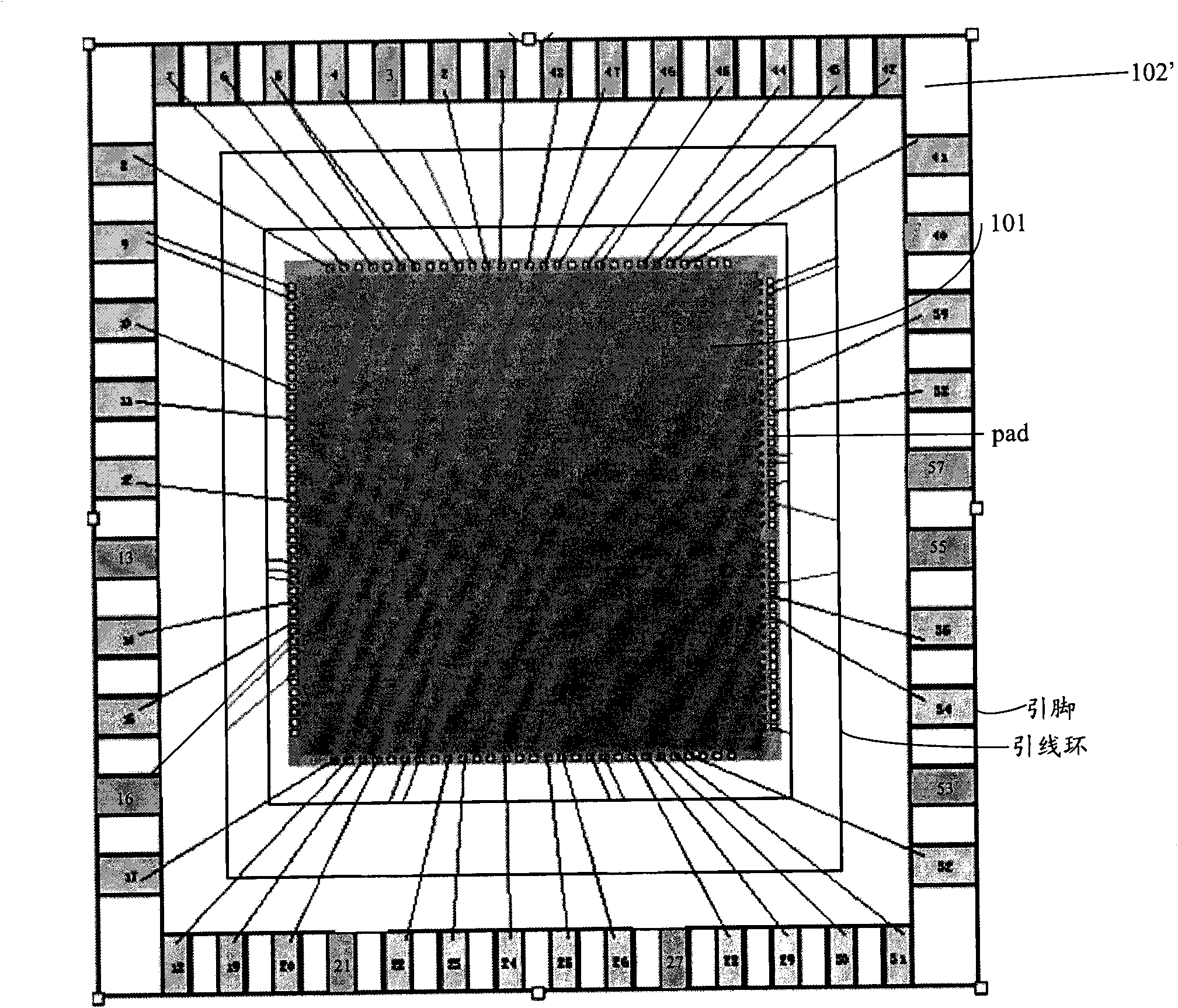
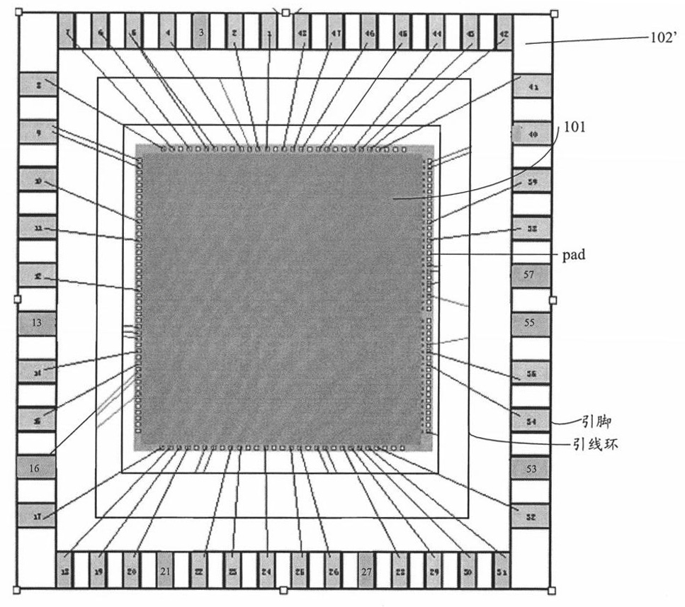
[0023] In order to solve the problem of insufficient pins on the lead frame 102 to wire all the contact pads on the chip, the present invention resets the lead frame. The lead frame includes a plurality of lead rings and a plurality of pins. The rings respectively surround the chip, and it is ensured that no electrical communication occurs between the multiple lead rings. When in use, when there are multiple pads with the same electrical characteristics on the chip, wire the pads with different electrical characteristics on the chip to different lead rings according to the different electrical characteristics of the pads, that is, there are multiple sets When connecting pads with different electrical characteristics, wire each group of pads with di...


PUM


Abstract

The invention discloses a lead frame for carrying out ceramic double in-line package (CDIP) on chips. The lead frame comprises multiple through collars and multiple pins, wherein the multiple through collars surround the chips respectively, and are separated from each other by insulating materials; multiple electropads with the same electrical characteristic on the chips are wired to the same through collar; when electropads with different electrical characteristics are arranged, each group of the electropads with different electrical characteristics is respectively wired to different through collars; and the different through collars are respectively connected into the different pins in one-to-one correspondence. The lead frame has the following advantages: the problem that the electropads can not be totally led out due to shortage of the pins on the lead frame 102 can be solved; and the manufacturing cost is not increased and the package cycle is not prolonged.

Description

Technical field [0001] The invention relates to semiconductor manufacturing technology, in particular to a lead frame for ceramic dual-in-line packaging of chips. Background technique [0002] In some engineering tests of semiconductor devices, such as electrostatic discharge (ESD) testing, final testing (FT) or burn-in (BI) testing, it is necessary to package the already manufactured chips. Currently, ceramic dual in-line packaging (DIP, Dual In-Line) is often used, which has the advantages of short packaging time and low cost. [0003] figure 1 It is a schematic diagram of the existing packaging structure of a chip using a ceramic DIP method. As shown in the figure, it includes a chip 101 and a lead frame 102. There are multiple contact pads with different electrical characteristics on the edge of the chip 101. The wire method is connected to the pins in the lead frame 102 by gold wires. [0004] Currently, for different chips, the lead frame 102 is used to package the chip, that...

Claims


Application Information

Patent Timeline
Patent Type & Authority Applications(China)
IPC IPC(8): H01L23/495H01L21/60
CPCH01L2224/49171H01L2224/45144H01L2224/48247H01L2924/00014
Inventor 冯军宏刘云海
Owner SEMICON MFG INT (SHANGHAI) CORP
Why Eureka
Try Eureka