Liquid crystal display and substrate

A liquid crystal display and substrate technology, applied in the direction of instruments, nonlinear optics, optics, etc., can solve the problems of increasing the production time of the process, and achieve the effect of reducing the alignment time

Active Publication Date: 2011-04-06
BOE TECH GRP CO LTD +1
View PDF0 Cites 22 Cited by
  • Summary
  • Abstract
  • Description
  • Claims
  • Application Information

AI Technical Summary

Problems solved by technology

[0006] Usually, these processes are completed by using two steps of coarse alignment and fine alignment to identify separately, and the identification of the two steps will increase the process production time

Method used


Image

  • Liquid crystal display and substrate
  • Liquid crystal display and substrate
  • Liquid crystal display and substrate

Examples


Embodiment 1

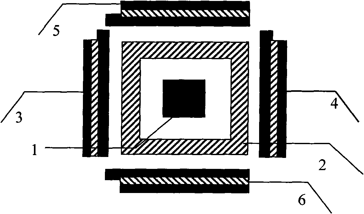
[0066] The liquid crystal display in this embodiment includes an array substrate and a color filter substrate, and combined alignment marks are provided on the array substrate and the color filter substrate, and the combined alignment marks include coarse alignment marks and fine alignment marks, The fine alignment mark is located in the peripheral surrounding area of ​​the coarse alignment mark;

[0067] The coarse alignment marks on the array substrate correspond to the coarse alignment marks on the color filter substrate;

[0068] The fine alignment marks on the array substrate correspond to the fine alignment marks on the color filter substrate.

[0069] figure 1 It is a structural schematic diagram of the alignment mark provided in the liquid crystal display of the present invention.

[0070] These include:

[0071] Coarse alignment marks (1) on the array substrate;

[0072] Coarse alignment marks (2) on the color filter substrate;

[0073] A fine alignment mark (3) ...

Embodiment 2

[0100] In this embodiment, the structure of the liquid crystal display is basically the same as that of the liquid crystal display in Embodiment 1. The difference is the design of the fine registration marks.

[0101] In this embodiment, the design of the fine alignment mark is as follows:

[0102] The fine alignment mark provided on the array substrate is composed of a rectangular initial alignment mark symbol and seven inverted L-shaped fine alignment mark symbols.

[0103] Wherein, the initial alignment mark symbol is positioned at the leftmost side of the fine alignment mark, and is longer than the rest of the alignment mark symbols, and the rest of the alignment mark symbols are equal in length (such as Figure 10 shown);

[0104] The fine alignment mark set on the color filter substrate consists of a rectangular initial alignment mark symbol and seven L-shaped fine alignment mark symbols.

[0105] Wherein, the initial alignment mark symbol is positioned at the far rig...


PUM

PropertyMeasurementUnit
widthaaaaaaaaaa
widthaaaaaaaaaa

Abstract

The invention discloses a liquid crystal display and a substrate. The invention aims at solving the problem that the substrate positioning of the existing products with substrates, particularly the liquid crystal display, requires long time. The liquid crystal display comprises an array substrate and a color film substrate, wherein the array substrate and the color film substrate are both provided with combination type positioning marks, each combination type positioning mark comprises a rough positioning mark and a fine positioning mark, and the fine positioning mark is located on the peripheral area of the rough positioning mark; the rough positioning mark of the array substrate corresponds to the rough positioning mark of the color film substrate; and the fine positioning mark of the array substrate corresponds to the fine positioning mark of the color film substrate. The invention can be applied to products related to substrate positioning, in particular to the liquid crystal display.

Description

technical field [0001] The invention belongs to the field of liquid crystal display manufacture and relates to the alignment of panels of liquid crystal displays. Background technique [0002] With the rapid development of science and technology, liquid crystal displays have been widely used in people's lives, such as TVs, computers, mobile phones, and various modern office equipment. [0003] The liquid crystal display manufacturing process involves identification, reading, and alignment of alignment marks (hereinafter referred to as Mark). For microelectronics / semiconductor manufacturing processes, the accuracy of Mark identification, reading, and alignment is particularly important. [0004] Usually, when making the panel, set the mark on the gate layer. When making a liquid crystal display panel, an array pattern is formed on a glass substrate, and the array pattern is generally recognized at the micron level. [0005] To ensure the formation of micron-level or even s...

Claims


Application Information

Patent Timeline
Patent Type & Authority Applications(China)
IPC IPC(8): G02F1/1333
CPCG02F1/1341G02F1/1333
Inventor 李于华曹昆
Owner BOE TECH GRP CO LTD
Why Eureka
Try Eureka