
Liquid crystal display and substrate thereof

Active Publication Date: 2011-03-03
BEIJING BOE OPTOELECTRONCIS TECH CO LTD +1
View PDF4 Cites 12 Cited by
  • Summary
  • Abstract
  • Description
  • Claims
  • Application Information

AI Technical Summary

Benefits of technology

[0071]The shape of the fine mark signs on the substrate may be of a rectangle shape, a reverse L shape, a triangle shape, a trapezoid shape or the like.
[0031]The liquid crystal display according to the embodiment of the present invention has the combination type mark. The steps for rough alignment and fine alignment can be carried out in a same process, so the separate identification steps for rough alignment and fine alignment in the conventionally technology can be avoided, and the alignment time can be reduced.

Problems solved by technology

In general, these processes are completed by two separate identifications steps for rough alignment and fine alignment, respectively, which increases the time required for performing the manufacturing processes.

Method used


Image

  • Liquid crystal display and substrate thereof
  • Liquid crystal display and substrate thereof
  • Liquid crystal display and substrate thereof

Examples


embodiment 1

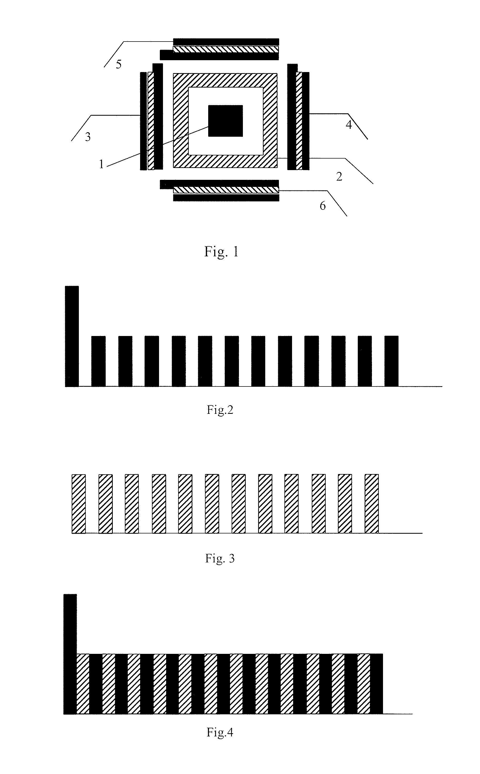
[0033]The liquid crystal display of the present embodiment comprises an array substrate and a color filter substrate. A combination type mark is disposed on each of the array substrate and the color filter substrate. The combination type mark comprises a rough mark and a fine mark that is located around the rough mark; the rough mark on the array substrate corresponds to the rough mark on the color filter substrate; the fine mark on the array substrate corresponds to the fine mark on the color filter substrate.

[0034]FIG. 1 is a structural schematic view showing the marks disposed in a liquid crystal display of the present embodiment after the array substrate and the color filter substrate are assembled together. These marks comprise: a rough mark 1 on the array substrate; a rough mark 2 on the color filter substrate; a fine mark 3 in an X direction and a fine mark 5 in a Y direction on a plane of the array substrate; a fine mark 4 in the X direction and a fine mark 6 in the Y direct...

embodiment 2

[0054]In the present embodiment, the structure of the liquid crystal display is substantially the same as that of the liquid crystal display in embodiment 1. The difference lies in the design of the fine marks.

[0055]In the present embodiment, the design of the fine mark is as follows.

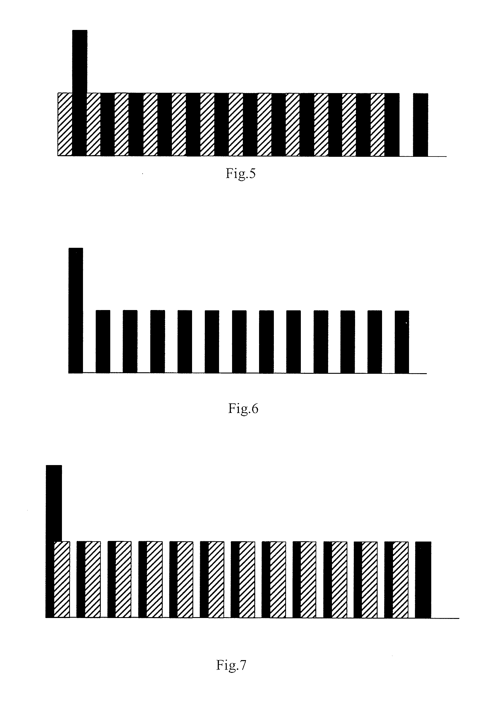
[0056]The fine mark disposed on an array substrate comprises one preceding mark sign of a rectangle shape and seven reverse L-shaped fine mark signs. The preceding mark sign is at the leftmost side of the fine mark and has a length larger than that of the rest mark signs, and the rest mark signs have an equal length (as shown in FIG. 10).

[0057]The fine mark disposed on the color filter substrate comprises one rectangle shaped preceding mark sign and seven L-shaped fine mark signs. The preceding mark sign is at the rightmost side of the fine marks and has a length larger than that of the rest mark signs, and the rest mark signs have an equal length (as shown in FIG. 11).

[0058]The bottom ends of the fine ...


PUM


Abstract

A liquid crystal display, comprising an array substrate and a color filter substrate, wherein a combination type mark is disposed on both of the array substrate and the color filter substrate, and the combination type mark comprises a rough mark and a fine mark that is located around the rough mark; and wherein the rough mark on the array substrate corresponds to the rough mark on the color filter substrate, and the fine mark on the array substrate corresponds to the fine mark on the color filter substrate.

Description

BACKGROUND[0001]Embodiments of the present invention pertain to manufacturing of a liquid crystal display (LCD).[0002]With rapid progress of technology, liquid crystal displays have been widely used in people's life, for example, applied to television sets, computers, mobile phones and various modern office appliances and the like.[0003]Manufacturing of a liquid crystal display generally involves identification, reading and alignment of alignment marks (referred to as “mark” hereinafter) and so on. Also in microelectronics / semiconductor manufacturing processes, identification, reading and alignment of marks are particularly important for the precision of the processes.[0004]In general, when a panel is formed, marks are disposed on a gate layer. When a liquid crystal display panel is manufactured, an array pattern is formed on a glass substrate, and the array pattern is usually performed with the micron level identification.[0005]In order to ensure the formation of micron-sized and e...

Claims


Application Information

Patent Timeline
IPC IPC(8): G02F1/1335
CPCG02F1/1341G02F1/1333
Inventor LI, YUHUACAO, KUN
Owner BEIJING BOE OPTOELECTRONCIS TECH CO LTD
Learn More