Exposure method

a technology of exposure apparatus and wafer, applied in the field of exposure method, can solve the problems of affecting the alignment accuracy, and reducing the efficiency of the exposure apparatus, so as to achieve the effect of improving the alignment accuracy of wafers

Active Publication Date: 2009-04-30
NAN YA TECH
View PDF1 Cites 13 Cited by
  • Summary
  • Abstract
  • Description
  • Claims
  • Application Information

AI Technical Summary

Benefits of technology

[0010]Accordingly, the present invention is directed to an exposure method capable of effectively improving the alignment accuracy of wafers.
[0011]The present invention is also directed to an exposure method to reduce the time needed by a photolithography process and thereby increase the throughput.
[0022]Since the present invention adopts a scheme including conducting a precise first alignment step on a wafer, followed by conducting a coarse second alignment step on the wafer and a photoresist exposure step. Therefore, the present invention is able to promote the alignment accuracy on the wafer to ensure the correctness of transferring a pattern.
[0023]In addition, the exposure method of the present invention uses an alignment tool independent from the exposure apparatus to conduct a precise first alignment step on the wafer, then uses the exposure apparatus to sequentially conduct a rough second alignment step prior to an exposure step on the wafer. Thus, the exposure apparatus is calibrated by a correlation between the result of the first alignment step and the result of the second alignment step, alignment accuracy of the exposure apparatus may be effectively promoted. Moreover, the number of the alignment marks measured by the exposure apparatus in the second alignment step is less than that in the first alignment step in the present invention. The independently disposed alignment tool and the exposure apparatus are able to simultaneously conduct the processes of themselves, and therefore, the exposure method of the present invention further reduces the alignment time of the exposure apparatus, so that the exposure apparatus can focus on conducting the photoresist exposure step to achieve a higher throughput.

Problems solved by technology

Since an exposure apparatus is unable to simultaneously conduct wafer alignment step and photoresist exposure step to meet the mass production requirement, the throughput of an exposure apparatus is much limited.
In particular, along with an continuously enhancement of device integration, more alignment marks measured on a same wafer are required to provide successive data for calibrating the exposure apparatus, which makes the situation of low throughput more serious.
In addition, in order to improve the above-mentioned low throughput problem of photoresist exposure, during conducting an pre-exposure alignment step with an exposure apparatus, it is very common to conduct alignment merely on a wafer chosen from a batch of wafers or several batches of wafers and then to calibrate the exposure apparatus by taking the alignment result obtained from aligning a single wafer as the base to align all wafers of a batch or several batches, which may more affect the alignment accuracy.
Since the accuracy in transferring a mask pattern onto the wafer is significant which directly affect the quality of a semiconductor process, how to effectively increase the throughput and promote the alignment accuracy to ensure higher quality of a photoresist pattern becomes one of important issues for the related manufactures to solve.

Method used


Image

  • Exposure method
  • Exposure method
  • Exposure method

Examples


Embodiment Construction

[0029]Reference will now be made in detail to the present preferred embodiments of the invention, examples of which are illustrated in the accompanying drawings. Wherever possible, the same reference numbers are used in the drawings and the description to refer to the same or like parts.

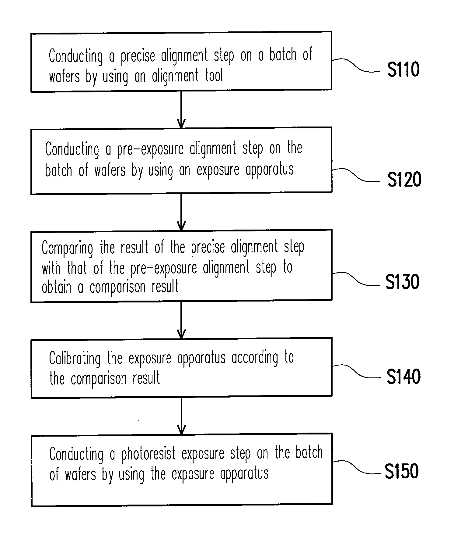
[0030]FIG. 1 is a flowchart of an exposure method according to an embodiment of the present invention. The exposure method is suitable for a photolithography process, wherein a photoresist layer has been formed on the surface of each wafer.

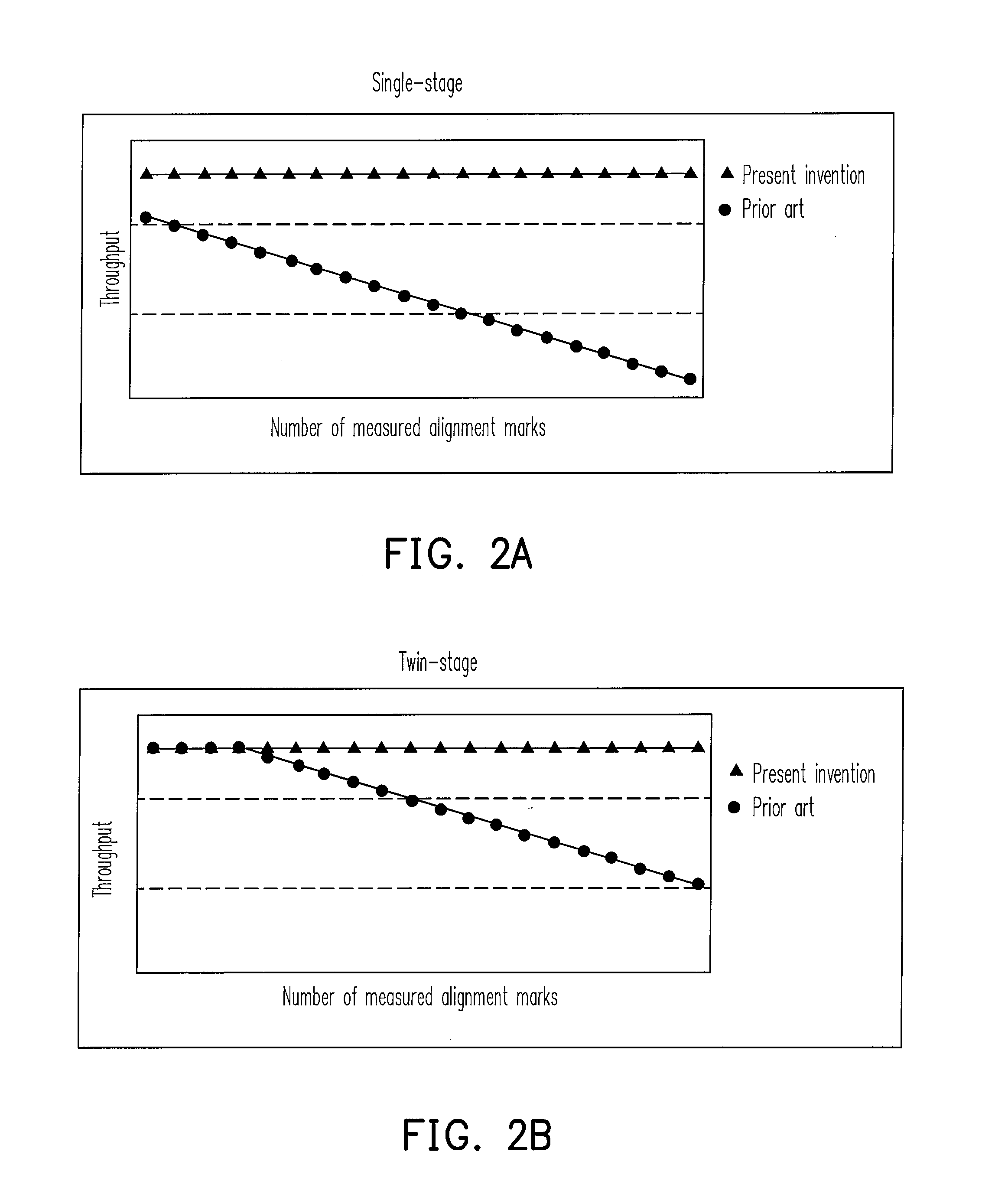
[0031]Referring to FIG. 1, first in step S110, an alignment tool is used to conduct a first alignment step, i.e. a precise alignment step, on a batch of wafers. The precise alignment step is, for example, performing a precise alignment measurement on each wafer of the batch. In other words, in the precise alignment step, the number of the alignment marks measured on a wafer ranges between 400 and 500.

[0032]The alignment tool used in step S110 is, for example, an of...


PUM

PropertyMeasurementUnit
semiconductoraaaaaaaaaa
timeaaaaaaaaaa
structureaaaaaaaaaa

Abstract

An exposure method suitable for a photolithography process is described. First, a wafer with a group of alignment marks formed thereon is provided. A first alignment step is conducted by using the group of the alignment marks on the wafer to obtain a first calibration data. Next, a second alignment step is conducted by using a portion of the group of alignment marks on the wafer to obtain a second calibration data. The first calibration data is then compared with the second calibration data to obtain a comparison result. Next, a photoresist exposure step is conducted on the wafer according to the comparison result.

Description

CROSS-REFERENCE TO RELATED APPLICATION[0001]This application claims the priority benefit of Taiwan application serial no. 96141052, filed on Oct. 31, 2007. The entirety of the above-mentioned patent application is hereby incorporated by reference herein and made a part of specification.BACKGROUND OF THE INVENTION[0002]1. Field of the Invention[0003]The present invention generally relates to a semiconductor process, and more particularly, to an exposure method suitable for a photolithography process.[0004]2. Description of Related Art[0005]Along with rapid progress of semiconductor process technology, further advancement in the operation speed and efficiency of semiconductor devices is demanded, which needs continuously increased compactness of a whole circuit component to increase the integration thereof. In general, in designing compact semiconductor devices, the photolithography process plays a significant role in the entire process.[0006]In a semiconductor process, the patterning...

Claims


Application Information

Patent Timeline
Patent Type & Authority Applications(United States)
IPC IPC(8): G03F7/20
CPCF15B2211/20515G03F7/70516G03F7/7085G03F9/7088G03F9/7011G03F9/7019G03F9/7046G03F9/7003
Inventor SHIH, CHIANG-LINCHEN, FENG-YICHO, KUO-YAO
Owner NAN YA TECH
Why Eureka
Try Eureka