Supercharge Your Innovation With Domain-Expert AI Agents!

Lead frame and chip package

A technology of chip packaging and lead frame, which is applied in the direction of semiconductor devices, semiconductor/solid-state device components, electric solid-state devices, etc., can solve the problem of reduced design flexibility of lead frames, and achieve the effect of large design flexibility

Active Publication Date: 2011-04-20
ADVANCED SEMICON ENG INC
View PDF4 Cites 2 Cited by
  • Summary
  • Abstract
  • Description
  • Claims
  • Application Information

AI Technical Summary

Problems solved by technology

Therefore, when designing a lead frame, it is necessary to increase the area of ​​the chip base for use as leads, so that the design flexibility of the lead frame is reduced.

Method used


Image

  • Lead frame and chip package
  • Lead frame and chip package
  • Lead frame and chip package

Examples


Embodiment Construction

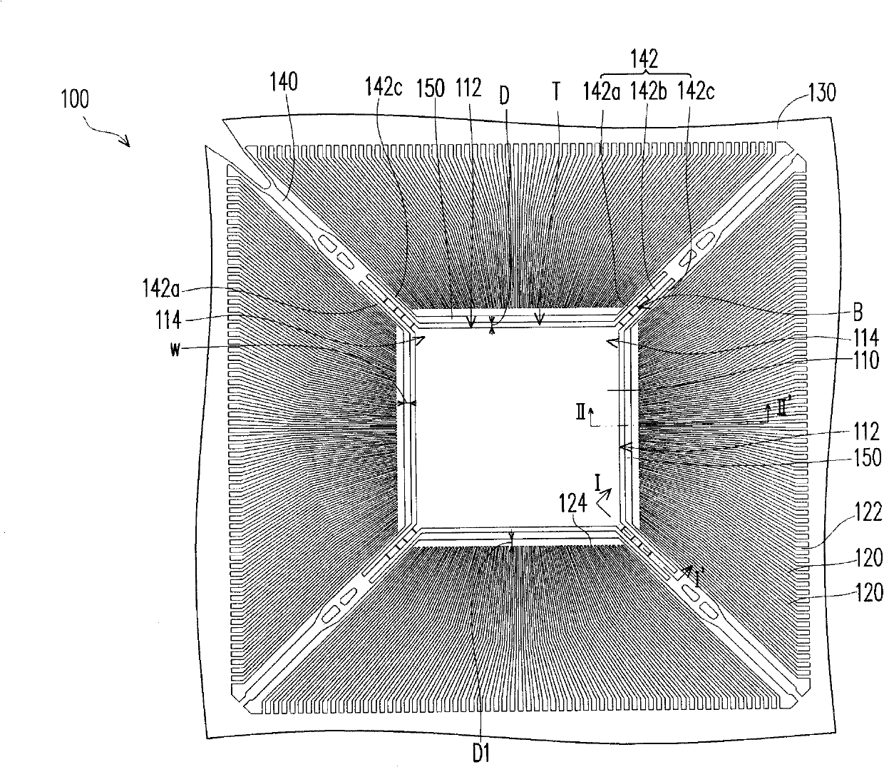
[0082] Figure 1A A top view of a lead frame according to an embodiment of the present invention is shown. Please refer to Figure 1A , the lead frame 100 of this embodiment includes a chip holder 110 , a plurality of pins 120 , an outer frame 130 , a plurality of connecting rods 140 and a plurality of grounding rods 150 . The pins 120 are arranged on the periphery of the chip holder 110, and the chip holder 110 and the pins 120 are arranged in the outer frame 130, wherein the end 122 of each pin 120 away from the chip holder 110 is connected to the outer frame 130, and each pin 120 One end 124 facing the die holder 110 is a free end.

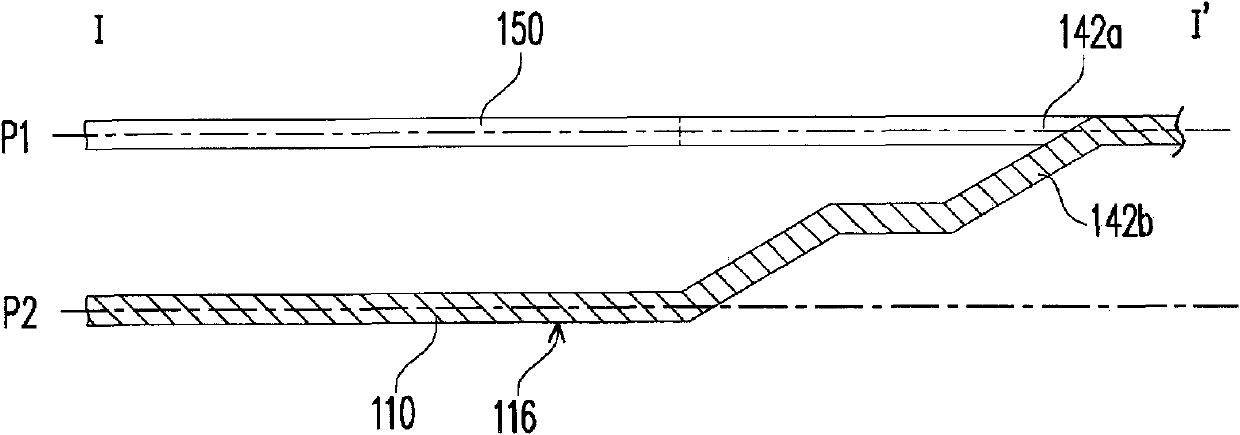
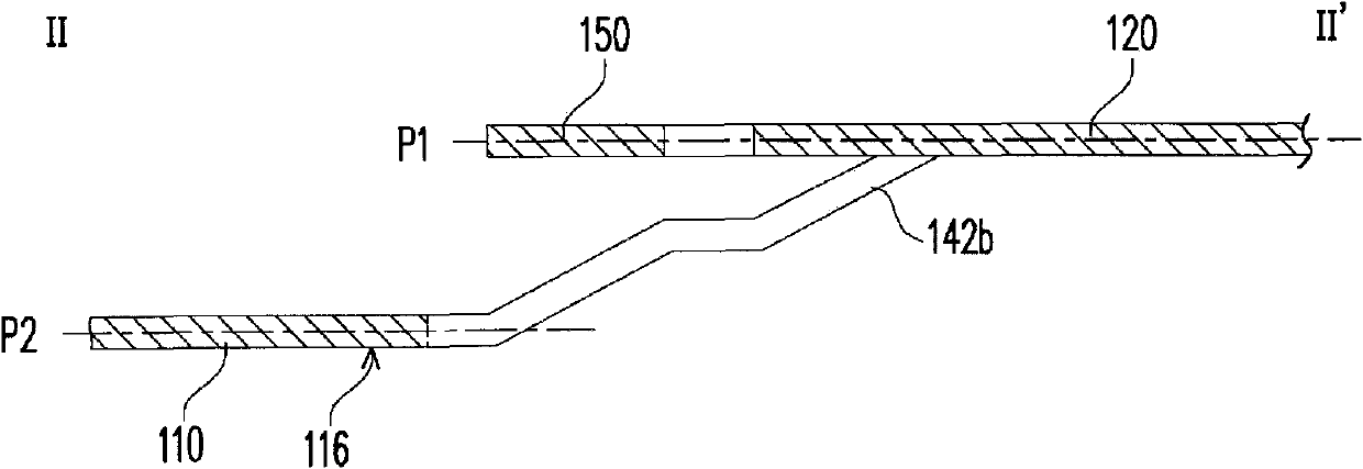
[0083] Each connecting rod 140 is connected to the outer frame 130 and has an end portion 142 extending toward the die holder 110 . The end portion 142 has a first branch 142 a , a second branch 142 b and a third branch 142 c parallel to each other, wherein the second branch 142 b is located between the first branch 142 a and the third branch ...


PUM


Abstract

The invention discloses a lead frame and a chip package. The lead frame comprises a chip base, a plurality of lead feet, an outer frame, a plurality of connecting rods and a plurality of grounding rods. The lead foot is disposed at the periphery of the chip base, the chip base and the lead foot are arranged in the outer frame, and one end of each lead foot far away from the chip base is connectedto the outer frame. Each connecting rod is connected to the outer frame and is provided with end parts extending towards the chip base, and the end part is provided with a first branch, a second branch and a third branch which are in parallel with each other. The second branch is disposed between the first and the third branch and is connected to the chip base. The grounding rod is disposed between the chip base and the lead feet. Each grounding rod is arranged along the periphery of each relative chip base, and a grounding rod is arranged between two adjacent connecting rods. Two ends of thegrounding rod are respectively connected to the first branch of the corresponding connecting rod and the third branch of the other connecting rod. The lead frame has quite a large design flexibility.

Description

technical field [0001] The invention relates to a lead frame and a chip package, and in particular to a lead frame in which a chip seat and a ground rod are separately arranged and a chip package using the lead frame. Background technique [0002] In the semiconductor industry, the production of integrated circuits (IC) can be mainly divided into three stages: IC design, IC process, and IC package. The packaging method of integrated circuits is to arrange the chip cut from the wafer on the carrier and electrically connect the chip to the carrier, and then cover the chip with molding compound to prevent the chip from being exposed to external temperature and moisture. influence and dust pollution, and provide a medium for electrical connection between the chip and the external circuit. [0003] The carrier is generally divided into a lead frame and a circuit board, and the lead frame has been widely used in chip packages in recent years because of its good heat dissipation e...

Claims


Application Information

Patent Timeline
IPC IPC(8): H01L23/495H01L23/13H01L23/58
CPCH01L2224/48091H01L2224/48247
Inventor 许月珍谢玫璘徐志宏陈光雄徐义程
Owner ADVANCED SEMICON ENG INC
Features
  • R&D
  • Intellectual Property
  • Life Sciences
  • Materials
  • Tech Scout
  • Unparalleled Data Quality
  • Higher Quality Content
  • 60% Fewer Hallucinations
Learn More