
Integrated circuit

A technology of integrated circuits and routing lines, applied in circuits, electrical components, electrical solid devices, etc., can solve problems such as cost and achieve the effects of large design flexibility, shortened time, and reduced internal impedance

Inactive Publication Date: 2015-11-11
NOVATEK MICROELECTRONICS CORP
View PDF4 Cites 3 Cited by
  • Summary
  • Abstract
  • Description
  • Claims
  • Application Information

AI Technical Summary

Problems solved by technology

However, changing the internal circuit layout of a chip means modifying multiple chip processing masks, which is expensive

Method used


Image

  • Integrated circuit
  • Integrated circuit
  • Integrated circuit

Examples


Embodiment Construction

[0146] The term "coupled" used throughout the specification (including claims) may refer to any direct or indirect means of connection. For example, if it is described in the text that a first device is coupled to a second device, it should be interpreted that the first device can be directly connected to the second device, or the first device can be connected through other devices or some kind of connection means. indirectly connected to the second device. In addition, wherever possible, elements, components, and steps with the same reference numerals are used in the drawings and embodiments to represent the same or similar parts. Components, components, and steps using the same symbols or using the same terms in different embodiments can refer to related descriptions.

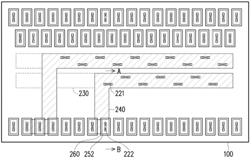
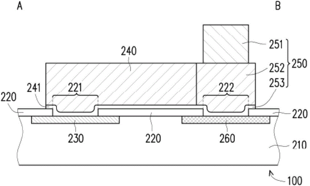
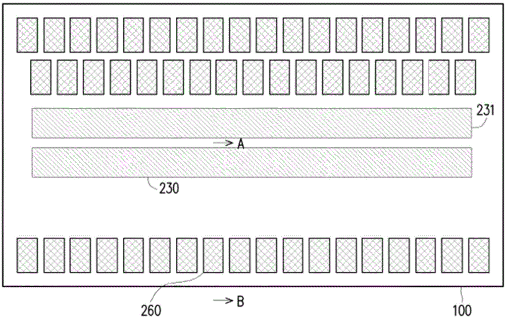
[0147] figure 1 It is a schematic top view illustrating a layout structure of an integrated circuit 100 according to an embodiment of the present invention. figure 2 It is the description of the embodimen...


PUM


Abstract

An integrated circuit (IC) is provided. The IC includes a chip, a passivation layer, a first metal internal connection, a routing wire and a bonding area. The passivation layer is disposed on the chip, wherein the passivation layer has a first opening. The first metal internal connection is disposed under the passivation layer and disposed in the chip. The routing wire is disposed on the passivation layer, wherein a first end of the routing wire electrically connects to a first end of the first metal internal connection through the first opening of the passivation layer. The bonding area is disposed on the passivation layer, wherein the bonding area electrically connects to a second end of the routing wire.

Description

technical field [0001] The present invention relates to an integrated circuit. Background technique [0002] The longer the width (or length) of a chip, the longer its metal interconnection (metalline). For example, the high-resolution power driver chip of the liquid crystal display panel often suffers from a voltage drop problem inside the chip because of its long and narrow layout, which makes the length of the metal interconnection too long. The longer the length of the metal interconnection in the chip, the greater its resistance value, resulting in more obvious voltage drop problem. Pressure drop problems will result in slower operating speeds. The traditional solution is usually to add vias (Via) and metal layers (Metallayer) into the chip during the chip manufacturing process to reduce the internal impedance of the electrical path (such as the system voltage VDD or the ground voltage VSS). However, changing the internal circuit layout of a chip means modifying mult...

Claims


Application Information

Patent Timeline
Patent Type & Authority Applications(China)
IPC IPC(8): H01L23/522
CPCH01L23/525H01L23/5286H01L23/53238H01L23/53252H01L24/05H01L24/13H01L2224/0235H01L2224/02375H01L2224/02379H01L2224/03462H01L2224/0401H01L2224/05022H01L2224/05124H01L2224/05147H01L2224/05548H01L2224/05582H01L2224/05644H01L2224/05647H01L2224/05655H01L2224/05664H01L2224/13005H01L2224/13007H01L2224/13009H01L2224/13023H01L2224/13024H01L2224/13028H01L2224/13144H01L2224/13147H01L2224/13155H01L2224/13164H01L2924/00014H01L2924/2075H01L2924/20751H01L23/3171H01L23/528H01L23/53209H01L23/53228H01L23/53242H01L2224/05016H01L2224/05666H01L2224/13016H01L2924/01028H01L2924/01029H01L2924/01046H01L2924/01074H01L2924/01079H01L2924/0132H01L2924/14H01L2924/2064
Inventor 吕国源周文彬陈永胜
Owner NOVATEK MICROELECTRONICS CORP
Learn More