Housing, production method therefor and electronic device
A manufacturing method and housing technology, applied in the direction of electrical equipment shell/cabinet/drawer, electrical components, etc., can solve problems such as inability to properly polish and coat the surface, poor yield, and inability to remove
- Summary
- Abstract
- Description
- Claims
- Application Information
AI Technical Summary
Problems solved by technology
Method used
Image
Examples
no. 1 Embodiment approach
[0036] The first embodiment is a method of manufacturing an electronic device case formed by integrally molding a self-healing surface-processed film and a resin.
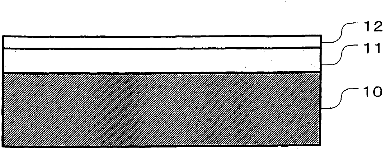
[0037] figure 1 It is a partial cross-sectional view of an electronic device case manufactured by the manufacturing method of the first embodiment. refer to figure 1 , The electronic device casing manufactured by the manufacturing method of the first embodiment has a main body resin 10 , a film base layer 11 , and a self-healing layer 12 .
[0038] The main body resin 10 is a resin component that constitutes the shape of the electronic device housing, and is made of PLA (polylactic acid, polylactic acid), ABS (Acrylonitrile Butadiene Styrene, acrylonitrile-butadiene-styrene copolymer), PC (polycarbonate, poly Carbonate), PC / ABS alloy (alloy) and other resins.
[0039] The film base layer 11 is integrally molded with the main body resin 10 in a state where a predetermined decorative layer is attached. The film b...
no. 2 Embodiment approach
[0048] image 3 It is a partial cross-sectional view of an electronic device case manufactured by the manufacturing method of the second embodiment. refer to image 3 , The electronic device casing manufactured by the manufacturing method of the second embodiment has a main body resin 10 and a self-healing layer 12 . The main body resin 10 and the self-healing layer 12 are made of the same materials as the main body resin 10 and the self-healing layer 12 constituting the case of the electronic device manufactured by the manufacturing method of the first embodiment.
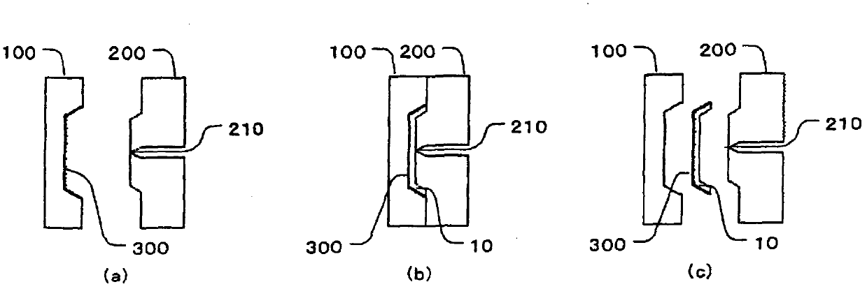
[0049] Figure 4 It is a figure explaining the manufacturing method of 2nd Embodiment. refer to Figure 4 , the electronic device housing manufactured by the manufacturing method of the second embodiment, due to the figure 2 The production method of the first embodiment described in hereinafter is also produced by injection molding, so the description will focus on the differences.
[0050] First, if Figure...
PUM
 Abstract
Description
Claims
Application Information
 - R&D
- Intellectual Property
- Life Sciences
- Materials
- Tech Scout
- Unparalleled Data Quality
- Higher Quality Content
- 60% Fewer Hallucinations
Browse by: Latest US Patents, China's latest patents, Technical Efficacy Thesaurus, Application Domain, Technology Topic, Popular Technical Reports.
© 2025 PatSnap. All rights reserved.Legal|Privacy policy|Modern Slavery Act Transparency Statement|Sitemap|About US| Contact US: help@patsnap.com


